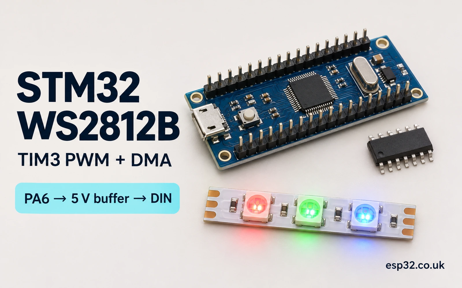
An STM32PriceAliExpress price can send WS2812BPriceAliExpress price data without a cycle-counted GPIO loop. In this esp32.co.uk/ guide, the STM32F103C8PriceAliExpress price Blue Pill uses TIM3 to generate 800 kHz PWM bit slots and DMA to feed each slot’s compare value. The output leaves PA6 at 3.3 V logic and passes through a 5 V SN74AHCT125 buffer before it reaches the strip. The lab drives up to 24 RGB pixels with one DMA buffer and leaves the line low between frames.
The example is designed around the Worldsemi WS2812B-2020 timing sheet linked below. It includes a complete CubeF1 HAL module, a three-colour bench pattern and timing checks for the first and last bits. The PWM output channel and the DMA request source serve different jobs. TIM3 channel 1 drives PA6, while TIM3 update events feed DMA1 channel 3. That choice makes the timing predictable even as the high time changes from bit to bit.
Identify the pixel and its timing sheet
Each RGB pixel receives 24 bits over a single data conductor referenced to ground. It consumes one pixel’s colour word and forwards later data to the next device. The order in the selected sheet is green, red, then blue, with the most significant bit first in every byte. Keep the application’s colour structure in the more familiar red, green and blue order if you like. The encoder can put the bytes on the wire in the order the pixel expects.
The waveform uses a short high pulse for zero and a long high pulse for one. Both fit a fixed 1.25 µs slot in this design. A continuous low interval at the end resets the serial reception and lets the LEDs display the newly received data. In the selected manufacturer sheet, reset requires more than 280 µs low. A zero bit has its own short high pulse, so the reset tail must be encoded as a compare value of zero for each period. Sending a row of logical zero bits would keep generating rising edges. Worldsemi WS2812B-2020 datasheet, copy hosted by M5Stack
Check the LED part and datasheet revision before using the compare constants. For example, the linked sheet lists a one-bit low interval of 220–420 ns. A separate manufacturer sheet distributed for the same family prints 580 ns to 1 µs in that row. Those are materially different windows. This lab uses the first sheet’s timing and checks the result at DIN. For a strip with a different confirmed part, calculate its compare values from its own timing, including the low half of each slot and the reset interval. Alternate Worldsemi WS2812B-2020 sheet hosted by Mouser
If the supplier provides only a generic WS2812 label, use a short sample and a logic capture before designing around it. Addressable strips can differ in channel order, bits per pixel and power arrangement. A 32-bit RGBW device changes the stride through the stream. A 12 V strip may group several physical LEDs into a single logical pixel and use a different controller. Inspect the supplier’s part information and input-end labels before treating those assemblies as a 24-bit, 5 V RGB strip.
Wire the strip and the logic buffer
Use a regulated 5 V supply for the strip and the SN74AHCT125. Give the Blue Pill a suitable separate power input and join its ground to the 5 V circuit ground. Run the LED supply and return directly to the strip so the LED current does not flow through the Blue Pill or the programmer ground wire. Follow the arrows printed on the strip to find the input end. Some assemblies print DI and DO instead. Connect the driver to DIN at the first pixel.
| Connection | Bench wiring |
|---|---|
| Blue Pill PA6 | SN74AHCT125 gate 1 input, pin 2 on the 14-pin package |
| SN74AHCT125 gate 1 enable | Pin 1, active low, tied to ground for this bench setup |
| SN74AHCT125 gate 1 output | Pin 3 through a 220 Ω series resistor to the first pixel DIN |
| SN74AHCT125 power | Pin 14 to 5 V, pin 7 to common ground |
| Buffer decoupling | 100 nF between pin 14 and pin 7, close to the package |
| First pixel power | 5 V and ground from the LED supply |
| Start-up input bias | 10 kΩ from gate 1 input to ground |
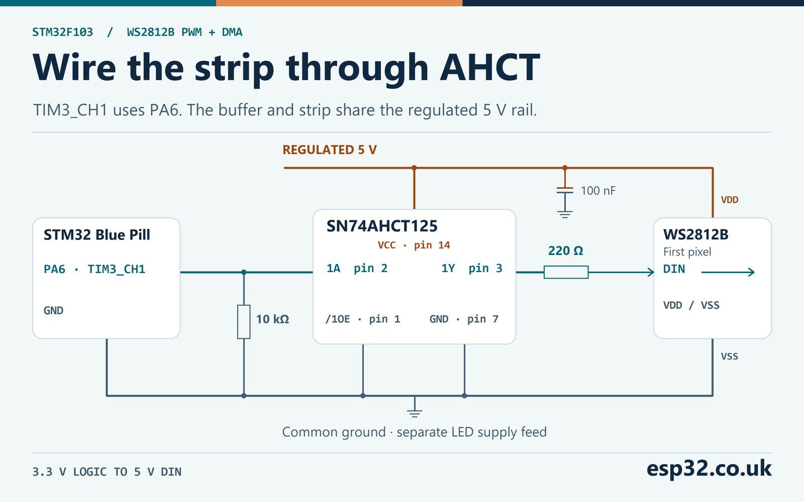
The selected pixel sheet specifies a minimum input-high voltage of 0.7 times its supply under the listed conditions. At 5 V that is 3.5 V, above a nominal 3.3 V logic high. The TI AHCT input accepts TTL-compatible levels, with a 2.0 V minimum input-high requirement in its recommended supply range. It translates the push-pull STM32 output to the strip’s logic domain. The output-enable input is active low. For unused gates, drive their output enables high and tie their input pins to a defined logic level. Keep their outputs open. TI SN74AHCT125 datasheet · STM32 GPIO voltage levels guide
The 10 kΩ pull-down holds the translator input low while PA6 is still an input during reset, provided the buffer is powered. During normal operation PA6 can drive it directly. The series resistor is a practical starting value for a short bench lead. Check the edge and ringing at the receiving pin and adjust the connection or resistance if necessary. A slow edge reduces the time spent above the receiving threshold, even if the duty cycle looks right on PA6. Keep the data lead close to its return and probe DIN with a short ground connection.
Use the strip’s stated current rating to size the supply. As a worked estimate, a strip budgeted at 45 mA per pixel would need about 1.08 A for 24 pixels at full output, before allowing margin for wiring loss and the controller. The value is illustrative because actual current depends on the LED revision, colour settings and strip construction. Start with the low-brightness pattern. If you later test bright white, measure voltage at the first and last pixels under that load. A 0.3 Ω round-trip feed at 1 A drops 0.3 V. Power distribution can affect both LED colour and the data thresholds seen by downstream pixels.
With the bench powered, first measure the two supply rails and the common ground connection. With the firmware idle, PA6 and the first DIN should be low. If the buffer input is low while its output is high, inspect the gate pinout, enable pin and supply before changing code. Power the buffer and strip together for this bench setup. If the system powers those domains independently, account for the state of DIN during ramp-up and power-down and check the powered-off input behavior of the actual components.
Keep the first tests physically small. One pixel on a short lead lets you verify the wiring and signal levels without much voltage drop. Move to a short strip segment only after that works. When extending the strip, compare the voltage at each injection point and the first pixel downstream. An ideal 5 V reading at the bench supply leaves the cable drop invisible. A supply with an adjustable current limit also lets you see whether the strip is pulling the source into current limiting when the displayed pattern changes. The LED rail can recover by the time a slow meter updates, so a scope on the rail is useful for intermittent flashes.
Derive the timer period and compare values
Set up the F103 with a nominal 72 MHz system clock and an AHB divider of one. In the lab, an 8 MHz HSE crystal feeds the PLL with a multiplier of nine. APB1 divides HCLK by two, so PCLK1 is 36 MHz. With an APB1 divider greater than one, TIM3 receives twice PCLK1 on this STM32F1. That gives a 72 MHz timer clock. The lab checks the 36 MHz APB1 setting and its divider before enabling the output. Confirm the crystal frequency and the project’s HSE configuration because software derives the nominal clock from those settings. ST RM0008 reference manual · STM32CubeMX and CubeIDE setup guide
The up-counter advances every 13.889 ns at a 72 MHz timer clock and prescaler zero. A 1.25 µs bit slot therefore takes 90 ticks. TIM3 counts from zero through ARR inclusive, so write 89 to ARR. In active-high PWM mode 1, the channel is high when CNT is below the active compare value. CCR1 of 22 gives 22 high ticks and 68 low ticks. CCR1 of 65 gives 65 high ticks and 25 low ticks. Compare zero holds the output low across the complete slot. STM32 timer and PWM guide
| Slot | CCR1 | High time at 72 MHz | Low time at 72 MHz | Selected timing window |
|---|---|---|---|---|
| Logical zero | 22 | 305.6 ns | 944.4 ns | High 220–380 ns, low 580–1000 ns |
| Logical one | 65 | 902.8 ns | 347.2 ns | High 580–1000 ns, low 220–420 ns |
| One reset-tail period | 0 | 0 ns | 1250 ns | Accumulate contiguous low periods |
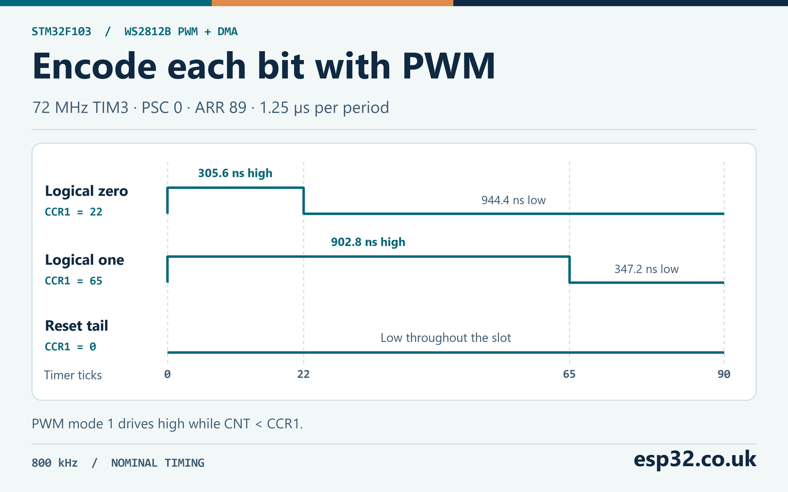
The common frequency mistake is to calculate ARR from PCLK1 and overlook the timer clock multiplier. If you used 45 ticks with the actual 72 MHz timer clock, the slot would be 625 ns. Conversely, leaving ARR at 89 while the timer actually runs at 36 MHz gives a 2.5 µs slot. Either error should be visible immediately between two adjacent rising edges in the data section. Changing the compare values alone cannot repair a wrong slot rate. Check both the period and the high and low widths.
Compare values are integers. If you port the lab to another clock, calculate the integer period and candidate compare counts, then recompute both edges in nanoseconds from those counts. At 48 MHz, for example, a 1.25 µs slot uses 60 ticks. Compare values 15 and 43 would produce high times of 312.5 and about 895.8 ns. Their low times would be 937.5 and about 354.2 ns. This is a worked alternative calculation. The supplied module deliberately accepts the stated 72 MHz setup so an accidental clock change becomes an explicit status.
The timer calculations describe the nominal digital output. Actual waveform measurements depend on the oscillator tolerance and the translator’s propagation and edge behavior. Use the first pixel’s local ground when measuring DIN. In a string that works with one pixel but fails under a heavier load, compare DIN again while the LEDs draw current. Ground bounce can shift the apparent signal levels seen by the receiver even when the timer period itself stays fixed.
The width numbers are far enough apart to diagnose the stream by inspection. The two nominal highs differ by about 597 ns. In a logic capture a threshold somewhere between them can separate the two groups, but the scope still needs to show that each group falls inside the receiver’s own high and low limits. At nominal clock the tighter zero-bit bound is the low interval, which is about 56 ns below the 1000 ns maximum. Record both widths if you are qualifying a new board or a long lead. A capture that merely decodes correctly on one bench run says little about the margin at the pixel.
Route update DMA to the CCR1 preload
PA6 is TIM3_CH1 with the default F103 pin map. Configure it for alternate-function push-pull. The module checks the TIM3 remap field and returns an error if another mapping is selected. The relevant DMA request is TIM3_UP on DMA1 channel 3. TIM3_CH1 capture/compare requests are on DMA1 channel 6. This lab uses the update request on channel 3, even though its destination is the channel 1 compare register. The selected request sets the pace and the destination address tells DMA what to write. ST STM32F103C8 datasheet · Blue Pill pinout guide
| Setting | Value |
|---|---|
| Output | TIM3 channel 1 on PA6, default remap |
| PWM | Up-counting mode 1, active high, ARR 89, PSC 0 |
| CCR1 preload | Enabled with OC1PE |
| DMA source request | TIM3 update, UDE in TIM3_DIER |
| DMA hardware channel | DMA1 channel 3 |
| Transfer | SRAM to TIM3_CCR1, 16-bit source and destination |
| Addressing | Increment source, hold destination fixed |
| Mode | Normal, polling full transfer, high priority |
At an update event the timer copies the current CCR1 preload into the active compare register. The event also requests a DMA transfer. The transfer arrives afterward and writes a new value into the preload for the following period. That separation is important. A write made directly to an active compare partway through a period could change the current pulse. With preload, the output holds its selected compare for the whole slot and the next slot begins at a predictable timer boundary. The DMA must still deliver the next value before the following update.
The DMA request uses the fixed STM32F103 channel mapping. SPI1 TX, USART3 RX, TIM1_CH2 and TIM3_CH4 also appear on DMA1 channel 3. Keep their requests disabled on that channel for the duration of this lab. A single channel has one active source and destination configuration. Another enabled peripheral request routed to that channel can advance the same buffer at the wrong time. This is especially easy to miss when adding a display using SPI1 TX DMA to an otherwise working LED project. STM32 DMA setup and troubleshooting guide
The 16-bit transfer width describes the DMA’s reads from the compare array and writes to the timer. The CPU programs the DMA controller’s own registers with aligned 32-bit accesses, as the device errata specifies. If you add diagnostic flag handling, follow the errata guidance on the global flag. Clearing it while a channel is active can interfere with transfer-error handling. The supplied module lets the HAL own status flags and explicitly turns the request and channel off when polling ends. STM32F103 medium-density errata ES096
Using an update request also gives the DMA nearly the whole 1.25 µs period to fill the preload. With a request generated at the compare point, the time remaining before rollover varies with the pulse. In this example, a compare event at 65 ticks leaves just 25 ticks until the next update. The update-paced design avoids that variable deadline and works during the zero-compare reset tail. Traffic from other bus masters can still add latency, so check the DIN waveform when the rest of the application is active.
A common Cube example uses HAL_TIM_PWM_Start_DMA() with a channel DMA handle. This lab instead starts the PWM output with HAL_TIM_PWM_Start(), configures normal DMA explicitly and then enables TIM_DMA_UPDATE. The distinction affects both the request mapping and the lifecycle of the PWM output. If you adapt a project generated for channel 1 DMA, remove that configuration for this lab and confirm that only UDE is used. Inspect the timer DIER register and channel count while debugging instead of moving the source array to a different channel and assuming the timer will follow. ST STM32F1 timer HAL v1.1.10
Follow the first bit and the reset tail
The timer starts with zero in both the active compare and preload. The code enables PWM at zero compare and waits with the line low before any frame. To transmit, it fills the SRAM buffer, arms DMA and enables the update DMA request. The first eligible update still outputs a low period and writes bit zero of the buffer into the preload. Here bit zero means the first position in the buffer, which may encode either logic value. The next update transfers that preload into the active compare and emits the first data pulse.
| Timer boundary | Active compare after update | What the DMA writes into preload |
|---|---|---|
| First update after UDE | 0, line stays low | First data compare |
| Next update | First data compare | Second data compare |
| Boundary starting the last data slot | Last data compare | First tail zero |
| Next update | First tail zero | Second tail zero |
| Boundary requesting the last DMA write | Penultimate tail zero | Final tail zero |
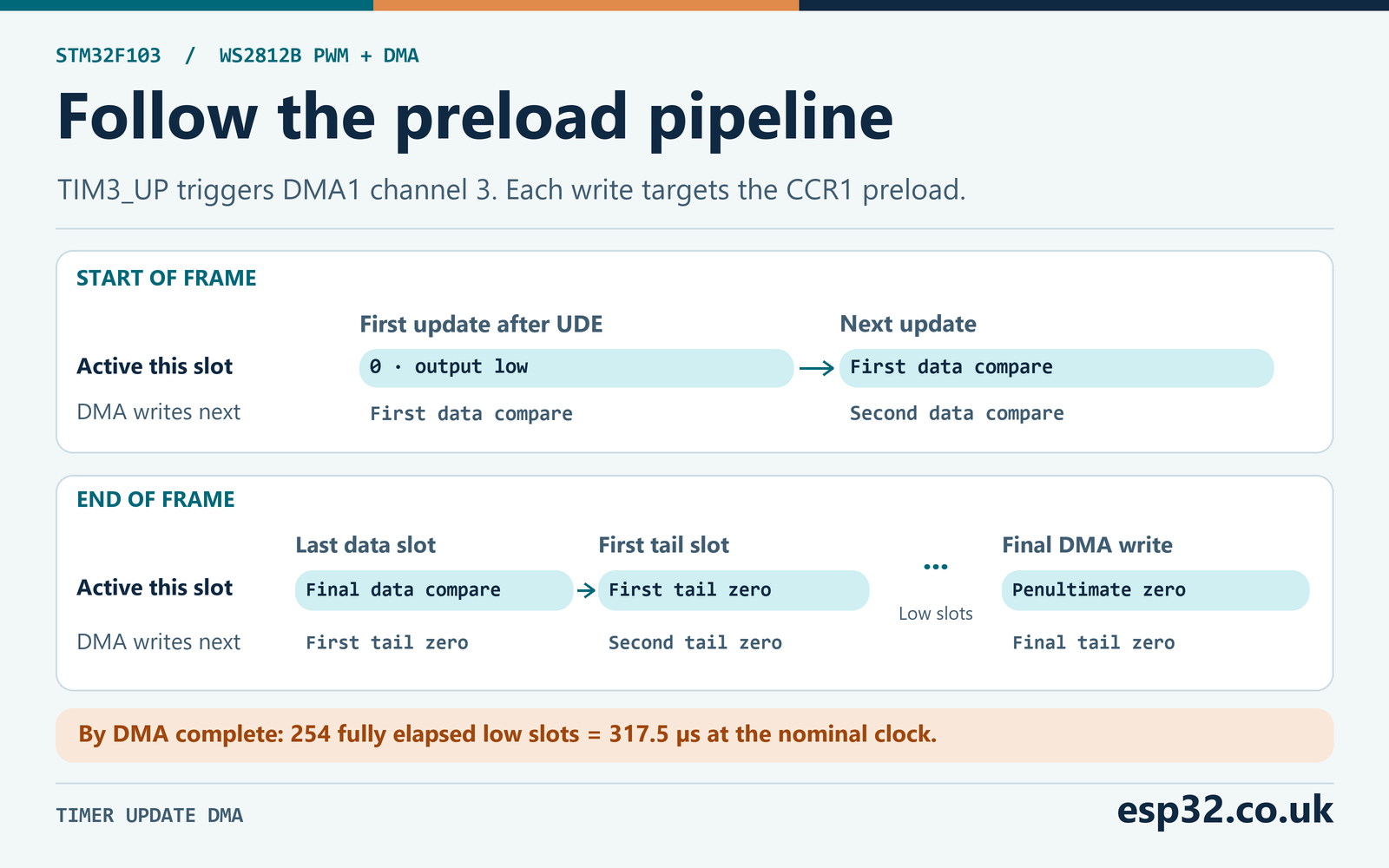
The DMA completion flag describes the last memory-to-peripheral write. It does not mark the instant at which the last written value starts a PWM period. Here the distinction is harmless because both the active and preloaded values are already zero by completion. With 256 zero entries at the end of the buffer, at least 254 complete all-low timer periods have elapsed when DMA writes the final zero, assuming each write completes before the next update. That is 317.5 µs of complete low slots, plus the final data bit’s low portion. The last zero remains in preload and the timer keeps PA6 low after the request is disabled.
Counting the reset tail from the last rising edge would also include the high portion of the last data bit, so use the last falling edge when checking the actual low interval on the scope. The next frame has its own startup preload delay. At low update rates the line stays low for much longer than the protocol requires. For a back-to-back test, call Ws_Show() again after the previous call returns. The line remains low while the CPU builds the next buffer and while the first compare moves through preload.
For 24 pixels, the data section has 576 bit slots and lasts 720 µs. The DMA buffer adds 256 zero entries, giving 832 transfers. The sum of data duration and nominal tail entries is 1.04 ms. The API’s elapsed wall time also includes encoding, arming, the initial wait for an update and polling. A measured interval from one frame’s first rising edge to the next frame’s first rising edge includes every gap between those calls. These times answer different questions, so state which interval you are comparing when reporting a maximum refresh rate.
The reset budget can be worked out from the completion boundary. More than 280 µs at a nominal 1.25 µs per slot means 224 exact periods would just reach the stated threshold. Add at least one for a strictly longer interval and allow for the two entries that can still be active or staged at DMA completion. Then add margin for the clock and receiving edge. The chosen 256 entries leave 37.5 µs above 280 µs even if you count only the 254 fully elapsed low periods. A tail chosen by dividing the reset duration by the slot time alone would miss both the strict threshold and the preload pipeline.
Add the HAL module to a CubeF1 project
Create an STM32F103C8 project with Serial Wire debug and the 72 MHz clock tree described above. Keep the generated HAL tick. Ensure the HAL GPIO, TIM, RCC and DMA modules are available to compile and link. Leave TIM3, PA6 and DMA1 channel 3 unassigned in generated code because this module owns their configuration. Copy the supplied header to the project’s include directory and the C file to the sources. If the IDE manages the HAL source files based on enabled peripherals, include the matching TIM and DMA drivers and enable the corresponding HAL modules in the project configuration.
The module first drives PA6 low as a GPIO. It configures normal DMA and PWM, explicitly enables CCR1 preload and generates a software update with DMA requests off. The output is then started at zero compare and PA6 switches to the timer’s alternate function. The one-millisecond startup wait establishes a reset interval before any colour data. Ws_Show() is a foreground blocking call. DMA and the timer generate the waveform while the CPU polls the HAL driver. Interrupts remain enabled, and the tick provides the timeout. ST STM32F1 DMA HAL v1.1.10
#ifndef WS2812_LAB_H
#define WS2812_LAB_H

#include <stddef.h>
#include <stdint.h>

enum { WS_MAX_PIXELS = 24 };

typedef struct {
    uint8_t red, green, blue;
} WsRgb;

typedef enum {
    WS_OK, WS_ARGUMENT, WS_CLOCK, WS_PIN, WS_INIT, WS_DMA, WS_TIMEOUT
} WsStatus;

/* Call after HAL_Init and system clock setup, with the HAL tick running. */
WsStatus Ws_Init(void);

/* Foreground only. This module owns TIM3, PA6 and DMA1 channel 3. */
WsStatus Ws_Show(const WsRgb *pixels, size_t count);

#endif
#include "ws2812_lab.h"
#include "stm32f1xx_hal.h"
enum { PERIOD_TICKS = 90, ZERO_TICKS = 22, ONE_TICKS = 65, RESET_SLOTS = 256 };
static uint16_t slots[WS_MAX_PIXELS * 24U + RESET_SLOTS];
static TIM_HandleTypeDef timer;
static DMA_HandleTypeDef dma;
static uint8_t ready;
static int clock_ok(void)
{
return HAL_RCC_GetPCLK1Freq() == 36000000U &&
(RCC->CFGR & RCC_CFGR_PPRE1) == RCC_CFGR_PPRE1_DIV2;
}
WsStatus Ws_Init(void)
{
if (!clock_ok()) {
return WS_CLOCK;
}
if (ready) {
return WS_OK;
}
__HAL_RCC_AFIO_CLK_ENABLE();
if (AFIO->MAPR & AFIO_MAPR_TIM3_REMAP) {
return WS_PIN;
}
__HAL_RCC_GPIOA_CLK_ENABLE();
__HAL_RCC_DMA1_CLK_ENABLE();
__HAL_RCC_TIM3_CLK_ENABLE();
__HAL_RCC_TIM3_FORCE_RESET();
__HAL_RCC_TIM3_RELEASE_RESET();
HAL_GPIO_WritePin(GPIOA, GPIO_PIN_6, GPIO_PIN_RESET);
GPIO_InitTypeDef pin = {
.Pin = GPIO_PIN_6, .Mode = GPIO_MODE_OUTPUT_PP,
.Speed = GPIO_SPEED_FREQ_HIGH, .Pull = GPIO_NOPULL
};
HAL_GPIO_Init(GPIOA, &pin);
dma.Instance = DMA1_Channel3;
dma.Instance->CCR = 0U;
dma.Init.Direction = DMA_MEMORY_TO_PERIPH;
dma.Init.PeriphInc = DMA_PINC_DISABLE;
dma.Init.MemInc = DMA_MINC_ENABLE;
dma.Init.PeriphDataAlignment = DMA_PDATAALIGN_HALFWORD;
dma.Init.MemDataAlignment = DMA_MDATAALIGN_HALFWORD;
dma.Init.Mode = DMA_NORMAL;
dma.Init.Priority = DMA_PRIORITY_HIGH;
timer.Instance = TIM3;
timer.Init.Prescaler = 0U;
timer.Init.CounterMode = TIM_COUNTERMODE_UP;
timer.Init.Period = PERIOD_TICKS - 1U;
timer.Init.ClockDivision = TIM_CLOCKDIVISION_DIV1;
timer.Init.AutoReloadPreload = TIM_AUTORELOAD_PRELOAD_ENABLE;
const TIM_OC_InitTypeDef channel = {
.OCMode = TIM_OCMODE_PWM1, .Pulse = 0U,
.OCPolarity = TIM_OCPOLARITY_HIGH, .OCFastMode = TIM_OCFAST_DISABLE
};
if (HAL_DMA_Init(&dma) != HAL_OK || HAL_TIM_PWM_Init(&timer) != HAL_OK ||
HAL_TIM_PWM_ConfigChannel(&timer, &channel, TIM_CHANNEL_1) != HAL_OK) {
return WS_INIT;
}
SET_BIT(TIM3->CCMR1, TIM_CCMR1_OC1PE);
SET_BIT(TIM3->CR1, TIM_CR1_URS);
TIM3->EGR = TIM_EGR_UG;
if (HAL_TIM_PWM_Start(&timer, TIM_CHANNEL_1) != HAL_OK) {
return WS_INIT;
}
pin.Mode = GPIO_MODE_AF_PP;
HAL_GPIO_Init(GPIOA, &pin);
HAL_Delay(1U);
ready = 1U;
return WS_OK;
}
static uint16_t *append_byte(uint16_t *dst, uint8_t value)
{
for (unsigned mask = 0x80U; mask != 0U; mask >>= 1U) {
*dst++ = (value & mask) ? ONE_TICKS : ZERO_TICKS;
}
return dst;
}
WsStatus Ws_Show(const WsRgb *pixels, size_t count)
{
if (!pixels || count == 0U || count > WS_MAX_PIXELS) {
return WS_ARGUMENT;
}
if (!ready) {
return WS_INIT;
}
if (!clock_ok()) {
return WS_CLOCK;
}
uint16_t *out = slots;
for (size_t i = 0; i < count; ++i) {
out = append_byte(out, pixels[i].green);
out = append_byte(out, pixels[i].red);
out = append_byte(out, pixels[i].blue);
}
for (unsigned i = 0; i < RESET_SLOTS; ++i) {
*out++ = 0U;
}
__DMB();
if (HAL_DMA_Start(&dma, (uintptr_t)slots, (uintptr_t)&TIM3->CCR1,
(uint32_t)(out - slots)) != HAL_OK) {
return WS_DMA;
}
__HAL_TIM_ENABLE_DMA(&timer, TIM_DMA_UPDATE);
HAL_StatusTypeDef result = HAL_DMA_PollForTransfer(&dma, HAL_DMA_FULL_TRANSFER, 10U);
__HAL_TIM_DISABLE_DMA(&timer, TIM_DMA_UPDATE);
__HAL_DMA_DISABLE(&dma);
if (result != HAL_OK) {
TIM3->CCR1 = 0U;
HAL_Delay(1U);
return (result == HAL_TIMEOUT || (HAL_DMA_GetError(&dma) & HAL_DMA_ERROR_TIMEOUT))
? WS_TIMEOUT : WS_DMA;
}
return WS_OK;
}Put the include and debugger variables in a generated user section. Put the initialization after the project’s clock setup and the refresh body inside its foreground loop. The example sends low-intensity red, green and blue to the first three pixels and black to the rest. For a single-pixel bench test, use a count of one and change that pixel’s colour between sends. Flash over SWD so the programmer does not share the waveform path. STM32CubeProgrammer flashing guide
#include "ws2812_lab.h"

volatile WsStatus led_status;
volatile uint32_t led_frames;

/* Place inside main, after HAL and clock initialization. */
static const WsRgb pixels[WS_MAX_PIXELS] = {
    {.red = 16}, {.green = 16}, {.blue = 16}
};
led_status = Ws_Init();
if (led_status != WS_OK) {
    for (;;) { __NOP(); }
}
for (;;) {
    led_status = Ws_Show(pixels, WS_MAX_PIXELS);
    if (led_status == WS_OK) {
        ++led_frames;
    }
    HAL_Delay(500);
}
Sending fewer entries than the physical strip length updates the initial part of the chain. For reliable whole-strip state, pass the actual pixel count and include explicit black entries where you want LEDs off. The lab bounds the count at 24, validates a null pointer or invalid count before touching the hardware and keeps the DMA source in static SRAM. Avoid calling the module concurrently or from an interrupt. It has one reusable buffer and depends on a running HAL tick. A different task must not mutate the caller’s colour data during encoding.
The STM32F1 HAL timeout path can return with the DMA hardware still enabled. The lab disables the timer’s DMA request and the DMA channel on every completed poll, including errors. On a failed poll it then writes zero to the compare preload and waits with the timer still running so zero becomes active. It checks both the HAL return status and the timeout flag because the v1.1.10 polling implementation can report a timeout through the handle’s error code. A transfer interrupted mid-frame can have changed some pixels. The next successful call sends a complete replacement frame. The returned status reports the transfer outcome, which is separate from what any individual LED displayed during recovery.
Check the status and frame counter together when bringing up the example. led_frames counts calls that successfully completed at the STM32. It gives you a quick way to distinguish a halted initialization from a stream of attempts. The WS2812B input has no acknowledgement to the driver, so a growing count can coexist with a disconnected DIN or an unpowered strip. Compare the count with what you see at the receiving pin and with the colour pattern. That separates a data transfer issue from an electrical connection issue without changing the timer parameters.
Verify the waveform before extending the strip
Start with a single pixel and probe PA6. Arm a capture for the first rising edge. You should see one contiguous block of data pulses followed by a flat low period. At 800 kHz the analyser needs enough sample rate to distinguish a high of roughly 306 ns from one of roughly 903 ns. Use an oscilloscope if you need voltage, ringing and threshold information. A protocol decoder can help count slots, but first verify which pulse widths its decoder interprets as zero and one.
Move the probe to the first DIN and repeat. The high level should now be in the buffer’s 5 V logic domain. Check the low level and high-time separation at the receiving pin. If the logic shape changes substantially across the buffer and the series resistor, inspect the buffer’s power, supply bypassing and output enable. Inspect the ground reference and the line loading too. A capture referenced to the controller ground alone can miss a voltage difference at the strip under load.
Decode a known first pixel. In the provided pattern the first RGB tuple is red 16, green 0, blue 0. The encoded bytes are 00 10 00 in GRB order. Binary 0x10 is 00010000, so one long pulse appears in the fourth position of the red byte, the twelfth slot overall when counted from one. This makes it easy to find the transition and check byte order. The next pixel sends 10 00 00, putting its long pulse in the fourth slot of its green byte. All other bits still have their short high pulse.
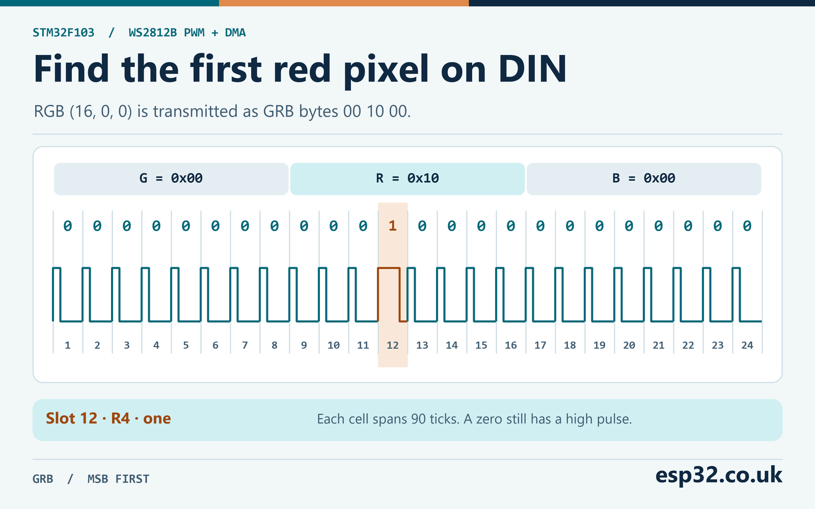
For the final-bit test, set the last pixel’s blue value to one and leave its remaining channels zero. Since blue goes last and is sent MSB first, the last data slot now has a long high pulse. Trigger and zoom near the tail. Confirm that the final long pulse has the same shape as a long pulse earlier in the capture and that it is followed by continuous low. This pattern exposes a missing last value more clearly than a frame ending in many all-zero pixel bytes.
| Symptom | Check |
|---|---|
No pulses and WS_CLOCK | HSE and PLL settings, PCLK1 and APB1 divide-by-two |
No pulses and WS_PIN | TIM3 remap and PA6 ownership |
WS_TIMEOUT | Timer counting, UDE, DMA1 channel 3 and the HAL tick |
| DMA success with no lights | Correct strip end, common ground, first DIN level and reset interval |
| Red and green swapped | Confirm the actual pixel byte order against the supplied pattern |
| One colour or pixel missing at the end | Count data slots and check the final compare and reset tail |
| Sparkles when a second peripheral runs | Channel 3 request conflicts, bus contention and supply noise |
| Works dimly and fails on bright white | Voltage drop, supply headroom, return routing and power injection |
The transfer counter can help locate a timing problem. In a halted or instrumented diagnosis, verify that DMA received a source address in SRAM, the peripheral address equals TIM3_CCR1 and the initial count equals 24 × pixels + 256. A counter that never decreases points to the request path. A decreasing count without the expected pin output points toward the timer’s output selection, preload, remap or GPIO configuration. Halting the core can itself affect the experiment depending on debug freeze configuration, so use a fresh uninterrupted capture for the final timing check.
When verifying a two-pixel chain, inspect the first pixel’s DOUT as well as DIN. On DIN the stream begins with the first pixel’s 24-bit word. At DOUT you expect the forwarded stream to begin with the next word once the first device has consumed its own. The two traces will be offset in time and may have different edge shapes because the pixel reshapes the signal. Decode them separately. This is a practical way to distinguish a broken connection between two pixels from a byte-order error in the firmware. If DOUT looks correct at one pixel and the next LED still misbehaves, probe the next DIN and compare its local ground.
Scale the frame with a memory and timing budget
Each additional pixel adds 24 halfwords, or 48 bytes, to the DMA buffer. The reset tail uses 512 bytes regardless of pixel count. The 24-pixel build therefore reserves 1,664 bytes for the compare stream. On the 20 KiB STM32F103C8, add the application’s stack, colour arrays and other buffers before increasing the cap. A hypothetical 150-pixel version of this same full-frame method would reserve 7,712 bytes for its DMA buffer and send 4.5 ms of colour data before the reset tail. It would need a fresh timeout and load assessment.
Circular DMA with half-buffer refill can reduce memory use for longer runs, but each refill has a hard deadline and needs a careful stop sequence. Start from a working normal-mode capture before making that change. Choose the interrupt priority and half-buffer size so the application can refill on time even when other interrupts are active. Verify a handoff between halves, the final data bit and the continuous reset low independently. The full-buffer lab keeps the entire frame available before sending it, which makes those boundaries easy to inspect.
Choose the frame rate from the application rather than simply calling the send function as fast as possible. A status display often has little to gain from refreshing hundreds of times a second. Sending only when values change leaves CPU time for other work. If periodic updates are important, measure the real call duration in the final firmware and budget for retries separately. Save the part revision, clock settings, buffer size and a representative DIN capture with the build so a replacement strip or clock change can be verified against the same setup.
For multiple callers, collect requested colours in application state and give one foreground task ownership of the hardware. That task can take a stable snapshot and call the blocking driver. A DMA-complete interrupt can free the CPU from polling in a later design. Even then, keep the source array reserved until completion and verify that the low reset budget is already met before starting another send. The reset tail in this version makes that handoff straightforward. A streaming implementation that stops immediately after the last data compare has to account for the active and preloaded values separately.