
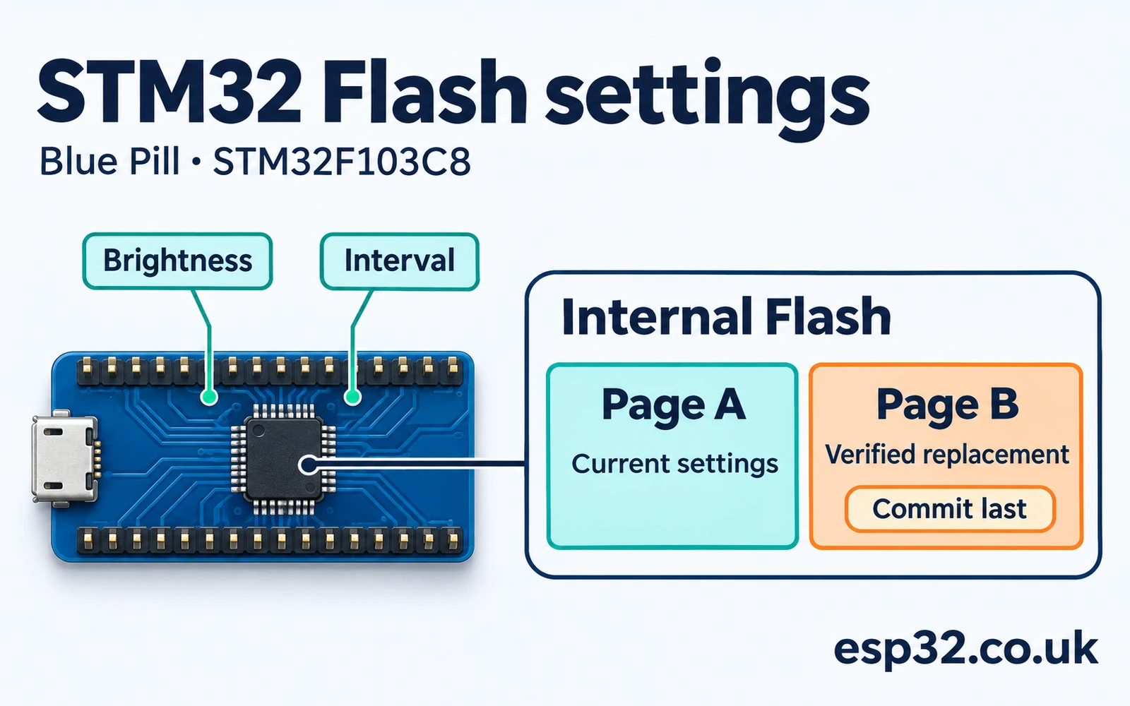
Settings such as a brightness level or a sampling interval belong in RAM while the application is running. To keep them after a power cycle, you need a persistent copy. On an STM32F103C8T6PriceAliExpress price Blue PillPriceAliExpress price, you can use part of the internal Flash for infrequent settings changes. The essential steps are to reserve the space in the linker script, respect page erase and halfword programming, and give the firmware a way to recognise a complete record at boot.
In this esp32PriceAliExpress price.co.uk/ guide, you will reserve two Flash pages and build a small settings store with STM32CubeF1 HAL. The application writes a new record to the alternate page, reads it back and writes its commit marker last. At startup it checks both pages and loads the newest valid record. The example stores brightness and an interval as numbers so you can verify the storage independently of any display or sensor.
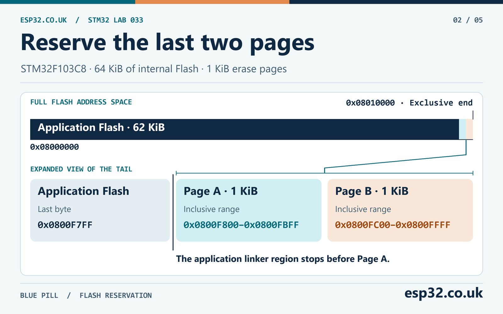
Quick answer. On a genuine 64 KiB STM32F103C8, limit the application linker region to 62 KiB and reserve pages starting at 0x0800F800 and 0x0800FC00. Use a one-page erase and aligned 16-bit writes. Keep the current record while you build and verify its replacement. Issue saves on explicit changes and load without writing at boot.
What Flash storage changes in your design
Flash is nonvolatile, so a saved record can survive a reset or removal of board power. Main Flash also holds the firmware. Your application needs a memory layout that gives code and settings separate regions. Choosing an address that happens to be empty today is unreliable, because a later build can grow into it.
For the STM32F103 medium-density Flash controller, the basic program operation writes a 16-bit halfword. A page erase affects a 1 KiB page on the C8. Erased bits read as ones, so an erased halfword reads 0xFFFF. Use the documented erase-before-program sequence. The controller’s normal programming rules are more restrictive than the general idea that a Flash bit can only be cleared by programming. This lab writes each slot halfword at most once after erase. ST PM0075, Main Flash programming and erase
| Storage choice | Useful for | Design cost |
|---|---|---|
| SRAM | Live settings, buffers and work in progress | Values need to be reloaded after reset |
| Internal Flash | Infrequently changed configuration | Page reservation, finite erase endurance and write latency |
| RTC backup registers | Small retained state when the backup domain stays powered | Capacity and retention depend on VBAT and reset conditions |
| External nonvolatile memory | Settings or logs that need different capacity or write endurance | Additional hardware, interface and failure handling |
Use the RTC backup domain when the retained data is small and the power arrangement supports it. Flash settings survive with VBAT disconnected because the cells store data without a supply. A firmware update or programmer erase can still remove them. Our earlier RTC guide covers the separate question of backup-domain retention. STM32 RTC and VBAT tutorial
The lab is a two-slot snapshot store. It replaces the entire settings record on a changed save. ST’s F1 EEPROM emulation application note describes a broader approach that appends variable records and transfers live data between pages. That style can amortise erase cycles across many updates. This lab uses one short snapshot per page so the recovery order and physical addresses are easy to inspect. ST AN2594, EEPROM emulation for STM32F10x
Reserve the last two pages in the linker script
Use a board you can erase and reflash for this experiment. Check its MCU marking and reported Flash size with your programmer. The STM32F103C8 part in this lab has 64 KiB of main Flash. The related CB density has 128 KiB, and other F1 variants can have different erase page geometry. Derive the addresses from the rated part you are using. A report of extra space on a clone does not establish the device’s electrical or endurance characteristics. ST STM32F103x8/xB datasheet
The 64 KiB region starts at 0x08000000 and ends just before 0x08010000. Subtract 2,048 bytes to get 0x0800F800. That leaves 63,488 bytes for the application, including code, constants and the Flash load image for initialised RAM variables.
| Region | First address | Last included address | Size |
|---|---|---|---|
| Application Flash | 0x08000000 | 0x0800F7FF | 62 KiB |
| Settings page A | 0x0800F800 | 0x0800FBFF | 1 KiB |
| Settings page B | 0x0800FC00 | 0x0800FFFF | 1 KiB |
| End marker | 0x08010000 | Exclusive boundary | No bytes |
Edit the active GNU linker script in the CubeIDE project. For a standard C8 project with 20 KiB of SRAM, replace its MEMORY block with the snippet below and place the symbol assignments and assertions after it. Keep the generated SECTIONS block, startup and stack settings. The settings addresses sit outside the shortened application Flash region.
/* Replace the standard 64 KiB C8 MEMORY block. Keep the existing SECTIONS. */
MEMORY
{
  RAM   (xrw) : ORIGIN = 0x20000000, LENGTH = 20K
  FLASH (rx)  : ORIGIN = 0x08000000, LENGTH = 62K
}

__settings_flash_start__ = ORIGIN(FLASH) + LENGTH(FLASH);
__settings_flash_end__ = ORIGIN(FLASH) + 64K;
ASSERT(__settings_flash_start__ == 0x0800F800, "Unexpected settings start")
ASSERT(__settings_flash_end__ == 0x08010000, "Unexpected flash end")
Check the linker’s selected script in the build configuration, especially if Debug and Release use different files. Inspect the map and the load addresses of every section that the programmer will write. In a typical generated project, the VMA for .data is in SRAM, while its initial values are loaded from Flash. A check that only looks at the run address of .data can miss a Flash load range that reaches into the reservation.
The linker assertions identify the expected geometry. The storage code also checks both exported boundary symbols and the device’s 16-bit Flash-size field before using the page addresses. These checks catch common mismatches. If your firmware uses a bootloader, an offset application, or a firmware update partition, review the complete partition map first. The lab layout assumes a standalone application starting at 0x08000000. ST CMSIS STM32F103 medium-density device definitions
An erase operation from the programming tool can bypass this reservation. When preserving settings across a firmware update, configure the updater to erase only the application pages and to write only the intended load ranges. Test that path before relying on it. The earlier flashing article covers the board’s programming interfaces. STM32CubeProgrammer and ST-LINK guide
Define a record the boot code can validate
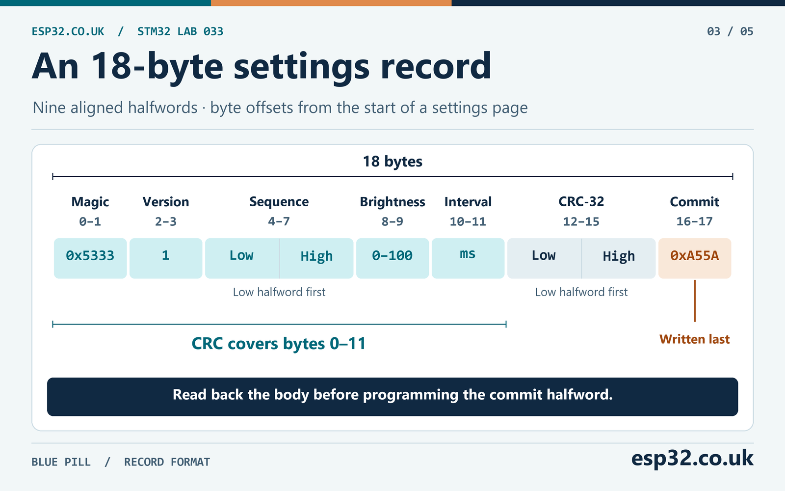
The stored representation is 18 bytes, arranged as nine halfwords. The fields are written in a defined order. The settings structure used by the rest of the C program is separate from this layout. Writing fields explicitly avoids relying on compiler padding, structure packing or a particular version of the application type.
| Bytes from page start | Field | Meaning |
|---|---|---|
| 0–1 | Magic 0x5333 | Identifies the lab record |
| 2–3 | Version 1 | Identifies the storage format |
| 4–7 | Sequence | 32-bit number, low halfword first |
| 8–9 | Brightness | Integer 0–100 |
| 10–11 | Interval | Integer 10–10,000 ms |
| 12–15 | CRC-32 | Covers bytes 0 through 11, low halfword first |
| 16–17 | Commit 0xA55A | Written last after body readback |
The CRC implementation consumes the low byte and then the high byte of each of the first six halfwords. It uses the reflected IEEE polynomial, starts at all ones and applies a final XOR of all ones. For the first record with sequence zero, brightness 25 and interval 1,000 ms, the CRC is 0x3443C2CB. You can use that value as a check when viewing the first save in a memory window.
The commit marker distinguishes a completed slot from a replacement whose body was interrupted. The loader also checks the magic, version, CRC and ranges. The CRC is an integrity check for accidental corruption. Keep credentials or data requiring authentication in a design with an appropriate security model.
Sequence numbers allow both pages to remain valid. If the unsigned difference between sequence B and sequence A is nonzero and less than half the 32-bit range, B is newer. The two valid slots in normal operation contain adjacent generations. When a save wraps from 0xFFFFFFFF to zero, the difference is still one. This comparison assumes the history was produced by the same alternating scheme.
An unsupported version is rejected by this reader. A later firmware needs a defined migration path if it changes the stored format or settings ranges. For an upgrade, read and validate the old layout before writing the new one to a known free page. Treat a deliberate format change as a data migration rather than a side effect of the first boot.
Add the STM32CubeF1 settings module
Create a C project for STM32F103C8Tx and retain Serial Wire debugging. Use the linker reservation above. Enable the Flash module in the project’s HAL configuration and include the Flash and FlashEx source files from the same STM32CubeF1 release as the rest of the project. Use a working HAL millisecond timebase. The code uses C11 and the STM32F103 medium-density device definitions.
Copy settings_store.h into Core/Inc and settings_store.c into Core/Src. Call the module from a single foreground owner. If several tasks can request settings updates, give one task ownership and pass it requests. A save unlocks the Flash controller for a defined operation, then locks it again. Concurrent writers would undermine the page selection and record order.
#ifndef SETTINGS_STORE_H
#define SETTINGS_STORE_H

#include <stdint.h>

typedef struct {
    uint16_t brightness;
    uint16_t interval_ms;
} Settings;

typedef enum {
    SETTINGS_OK,
    SETTINGS_EMPTY,
    SETTINGS_BAD_ARGUMENT,
    SETTINGS_BAD_LAYOUT,
    SETTINGS_FLASH_ERROR,
    SETTINGS_VERIFY_ERROR
} SettingsResult;

SettingsResult Settings_Load(Settings *settings);
SettingsResult Settings_Save(const Settings *settings);

#endif
The reader changes the caller’s settings only when a record passes validation. An empty result leaves the caller’s default values in place. A save checks the ranges and layout first. If the requested values match the current committed record, it returns successfully without an erase. Otherwise it uses the other page. The first save goes to A with sequence zero.
#include "settings_store.h"
#include "stm32f1xx_hal.h"
#include <stdbool.h>
#include <stddef.h>
#if !defined(STM32F103xB)
#error "This lab uses the STM32F103 medium-density device definitions."
#endif
#define PAGE_A UINT32_C(0x0800F800)
#define PAGE_B UINT32_C(0x0800FC00)
#define FLASH_END_EXCLUSIVE UINT32_C(0x08010000)
#define RECORD_MAGIC UINT16_C(0x5333)
#define RECORD_VERSION UINT16_C(1)
#define RECORD_COMMIT UINT16_C(0xA55A)
extern const uint8_t __settings_flash_start__[];
extern const uint8_t __settings_flash_end__[];
enum {
MAGIC, VERSION, SEQ_LO, SEQ_HI, BRIGHTNESS, INTERVAL,
CRC_LO, CRC_HI, COMMIT, RECORD_WORDS
};
typedef struct {
bool valid;
uint32_t sequence;
Settings settings;
} Slot;
_Static_assert(FLASH_PAGE_SIZE == 1024U, "Expected 1 KiB flash pages");
static bool layout_ok(void)
{
return (uintptr_t)__settings_flash_start__ == PAGE_A &&
(uintptr_t)__settings_flash_end__ == FLASH_END_EXCLUSIVE &&
*(const volatile uint16_t *)FLASHSIZE_BASE == 64U;
}
static bool values_ok(const Settings *settings)
{
return settings->brightness <= 100U &&
settings->interval_ms >= 10U && settings->interval_ms <= 10000U;
}
static bool same_values(const Settings *a, const Settings *b)
{
return a->brightness == b->brightness && a->interval_ms == b->interval_ms;
}
static uint32_t join_words(uint16_t low, uint16_t high)
{
return (uint32_t)low | ((uint32_t)high << 16);
}
static uint32_t record_crc(const uint16_t words[RECORD_WORDS])
{
uint32_t crc = UINT32_MAX;
for (size_t i = 0; i < CRC_LO; ++i) {
uint32_t word = words[i];
for (unsigned byte = 0; byte < 2U; ++byte) {
crc ^= word & 0xFFU;
word >>= 8;
for (unsigned bit = 0; bit < 8U; ++bit) {
uint32_t polynomial = (crc & 1U) ? UINT32_C(0xEDB88320) : 0U;
crc = (crc >> 1) ^ polynomial;
}
}
}
return crc ^ UINT32_MAX;
}
static Slot read_slot(uint32_t address)
{
Slot slot = {0};
const volatile uint16_t *flash = (const volatile uint16_t *)(uintptr_t)address;
if (flash[COMMIT] != RECORD_COMMIT) {
return slot;
}
uint16_t words[RECORD_WORDS];
for (size_t i = 0; i < COMMIT; ++i) {
words[i] = flash[i];
}
slot.sequence = join_words(words[SEQ_LO], words[SEQ_HI]);
slot.settings.brightness = words[BRIGHTNESS];
slot.settings.interval_ms = words[INTERVAL];
slot.valid = words[MAGIC] == RECORD_MAGIC && words[VERSION] == RECORD_VERSION &&
record_crc(words) == join_words(words[CRC_LO], words[CRC_HI]) &&
values_ok(&slot.settings);
return slot;
}
static uint32_t latest_page(const Slot *a, const Slot *b)
{
if (!a->valid) {
return b->valid ? PAGE_B : 0U;
}
if (!b->valid) {
return PAGE_A;
}
uint32_t difference = b->sequence - a->sequence;
return difference != 0U && difference < UINT32_C(0x80000000) ? PAGE_B : PAGE_A;
}
SettingsResult Settings_Load(Settings *settings)
{
if (settings == NULL) {
return SETTINGS_BAD_ARGUMENT;
}
if (!layout_ok()) {
return SETTINGS_BAD_LAYOUT;
}
Slot a = read_slot(PAGE_A);
Slot b = read_slot(PAGE_B);
uint32_t latest = latest_page(&a, &b);
if (latest == 0U) {
return SETTINGS_EMPTY;
}
*settings = latest == PAGE_A ? a.settings : b.settings;
return SETTINGS_OK;
}
static SettingsResult write_slot(uint32_t address, uint32_t sequence,
const Settings *settings)
{
uint16_t words[RECORD_WORDS] = {
[MAGIC] = RECORD_MAGIC,
[VERSION] = RECORD_VERSION,
[SEQ_LO] = (uint16_t)sequence,
[SEQ_HI] = (uint16_t)(sequence >> 16),
[BRIGHTNESS] = settings->brightness,
[INTERVAL] = settings->interval_ms,
[COMMIT] = RECORD_COMMIT
};
uint32_t crc = record_crc(words);
words[CRC_LO] = (uint16_t)crc;
words[CRC_HI] = (uint16_t)(crc >> 16);
FLASH_EraseInitTypeDef erase = {0};
erase.TypeErase = FLASH_TYPEERASE_PAGES;
erase.PageAddress = address;
erase.NbPages = 1U;
uint32_t page_error = UINT32_MAX;
if (HAL_FLASHEx_Erase(&erase, &page_error) != HAL_OK ||
page_error != UINT32_MAX) {
return SETTINGS_FLASH_ERROR;
}
const volatile uint16_t *flash = (const volatile uint16_t *)(uintptr_t)address;
for (size_t i = 0; i < RECORD_WORDS; ++i) {
if (flash[i] != UINT16_MAX) {
return SETTINGS_VERIFY_ERROR;
}
}
for (size_t i = 0; i < COMMIT; ++i) {
if (words[i] != UINT16_MAX &&
HAL_FLASH_Program(FLASH_TYPEPROGRAM_HALFWORD, address + 2U * i,
words[i]) != HAL_OK) {
return SETTINGS_FLASH_ERROR;
}
}
for (size_t i = 0; i < COMMIT; ++i) {
if (flash[i] != words[i]) {
return SETTINGS_VERIFY_ERROR;
}
}
if (HAL_FLASH_Program(FLASH_TYPEPROGRAM_HALFWORD, address + 2U * COMMIT,
RECORD_COMMIT) != HAL_OK) {
return SETTINGS_FLASH_ERROR;
}
Slot saved = read_slot(address);
return saved.valid && saved.sequence == sequence &&
same_values(&saved.settings, settings) ? SETTINGS_OK : SETTINGS_VERIFY_ERROR;
}
SettingsResult Settings_Save(const Settings *settings)
{
if (settings == NULL || !values_ok(settings)) {
return SETTINGS_BAD_ARGUMENT;
}
if (!layout_ok()) {
return SETTINGS_BAD_LAYOUT;
}
Slot a = read_slot(PAGE_A);
Slot b = read_slot(PAGE_B);
uint32_t latest = latest_page(&a, &b);
const Slot *current = latest == PAGE_A ? &a : &b;
if (latest != 0U && same_values(¤t->settings, settings)) {
return SETTINGS_OK;
}
uint32_t target = latest == PAGE_A ? PAGE_B : PAGE_A;
uint32_t sequence = latest == 0U ? 0U : current->sequence + 1U;
if (HAL_FLASH_Unlock() != HAL_OK) {
return SETTINGS_FLASH_ERROR;
}
SettingsResult result = write_slot(target, sequence, settings);
if (HAL_FLASH_Lock() != HAL_OK) {
return SETTINGS_FLASH_ERROR;
}
return result;
}The HAL calls in the lab are synchronous. HAL_FLASHEx_Erase() is configured for one page. HAL_FLASH_Program() receives one halfword at a time at an even address. The code checks that the record area is erased, verifies the body before committing and reopens the completed slot through the same reader used at boot. ST HAL Flash source v1.1.10, ST HAL FlashEx source v1.1.10
The module and tagged Flash drivers compiled for Cortex-M3, and a small link fixture placed code and the Flash load image of initialised RAM inside the 62 KiB region. An oversized text section was rejected by the linker. The fixture checks the linker geometry and integration of the C symbols. Build the complete CubeMX firmware and perform the bench procedure to test the board.
Save once and test a cold restart
Use the following integration in the named user-code sections of the generated main.c. The application leaves default values active unless it can load a valid record. The debugger request lets you trigger an explicit save while keeping Flash writes out of the ordinary loop path.
/* USER CODE BEGIN Includes */
#include "settings_store.h"
/* USER CODE END Includes */

/* USER CODE BEGIN PV */
volatile uint16_t active_brightness = 25U;
volatile uint16_t active_interval_ms = 1000U;
volatile uint16_t requested_brightness = 25U;
volatile uint16_t requested_interval_ms = 1000U;
volatile uint32_t settings_save_request;
volatile SettingsResult settings_load_result;
volatile SettingsResult settings_save_result = SETTINGS_EMPTY;
/* USER CODE END PV */

/* USER CODE BEGIN 2: after HAL and clock initialisation */
Settings restored;
settings_load_result = Settings_Load(&restored);
if (settings_load_result == SETTINGS_OK) {
    active_brightness = restored.brightness;
    active_interval_ms = restored.interval_ms;
}
/* USER CODE END 2 */

/* Inside the existing while (1) body, in a USER CODE section */
if (settings_save_request != 0U) {
    settings_save_request = 0U;
    Settings proposed = {requested_brightness, requested_interval_ms};
    settings_save_result = Settings_Save(&proposed);
    if (settings_save_result == SETTINGS_OK) {
        active_brightness = proposed.brightness;
        active_interval_ms = proposed.interval_ms;
    }
}
Build and flash the project after inspecting its map. On a blank reservation, confirm that the load result is SETTINGS_EMPTY and the active defaults are 25 and 1,000. If the reservation already has a valid record from an earlier run, the loader will use it. Hold the core at an ordinary breakpoint outside any Flash operation, enter values in the requested variables, set the request to 1 and resume. Wait for the save to finish before halting again.
| Test | Expected outcome |
|---|---|
| First save on blank pages | A contains sequence zero and commit 0xA55A |
| Save changed settings | B gets sequence one and A remains valid |
| Save the same settings again | No new sequence and no page erase |
| Save a brightness above 100 | Invalid argument result, existing record intact |
| Reset without reflashing | Load the last committed settings |
| Remove and restore board power | Load the same settings after cold boot |
The request is a bench interface. In an application it could come from a deliberate menu action or a validated serial command. Read and validate the complete command before converting it to the smaller stored field types. Preserve the save result so the user interface can distinguish a value held in RAM from one committed to Flash. STM32 UART and HAL tutorial
Read the first record in the debugger
After the first successful save with the default values, open a memory view at 0x0800F800 and display 18 bytes. If the debugger displays a larger range, mark the end of the record before comparing the values. Only bytes 0 through 17 belong to this format. In a freshly erased page the rest should read as FF. The next saved record belongs at the start of B, one full page away.
| Address in A | Bytes in increasing address order | Interpretation |
|---|---|---|
| 0x0800F800 | 33 53 01 00 | Magic and version |
| 0x0800F804 | 00 00 00 00 | First sequence |
| 0x0800F808 | 19 00 E8 03 | Brightness 25 and interval 1,000 ms |
| 0x0800F80C | CB C2 43 34 | CRC-32 0x3443C2CB |
| 0x0800F810 | 5A A5 | Committed record |
Read the byte order before interpreting a word view. A 32-bit little-endian display of the first four bytes will show 0x00015333. That value combines the magic and version into one display item. A 16-bit view shows the two fields separately. A memory window can also retain a previous snapshot while the target runs, so refresh it after stopping the core again.
Save a second record with brightness 80 and interval 250. The first slot should retain its original values, and the second should show sequence one and the new settings. Reboot the existing firmware and check that active_brightness and active_interval_ms now show 80 and 250. A download-and-debug action may reprogram Flash as it starts. Use a plain reset or attach to the running target for the persistence check. For the cold-boot case, remove every active power source including a USB cable or probe connection that supplies the board, then start the installed firmware again.
Decide when the application reports a save
Think of the settings as three pieces of state. The user interface has a candidate, the application has its current runtime values, and the storage module has a committed snapshot. The debugger integration applies the candidate to runtime only after success. If your application previews changes before saving, show the preview immediately and keep a separate dirty flag until the save succeeds. When a write fails, preserve the pending values in RAM so the user can retry or choose to discard them.
Capture the complete settings object before calling the module. For example, a UART receiver may assemble a command across several interrupts. Queue the complete command to the foreground, parse both fields, validate their ranges and then pass a local Settings value to Settings_Save(). This keeps the candidate stable through the CRC calculation and programming. It also keeps the Flash work out of the receive interrupt.
Handle numeric conversion before narrowing the values. A command with interval 65,546 would become 10 if cast straight to an unsigned 16-bit field. The module would see a valid 10 ms interval and could save it. A serial parser should reject out-of-range input in the wider parsed type, then convert only after validation. Apply the same rule to negative values, integer overflow and partially parsed strings.
If the application receives a save request while another is pending, choose a policy at the application boundary. A menu can disable its Save button while busy. A remote protocol can queue one complete candidate and reply with a busy state for further requests. With a deferred save, report the durable result after the write and readback, even if the interface acknowledged reception earlier. If the device resets before reporting a result, load the stored settings on reconnect and let the client compare them with the requested values.
Understand which page survives an interrupted save
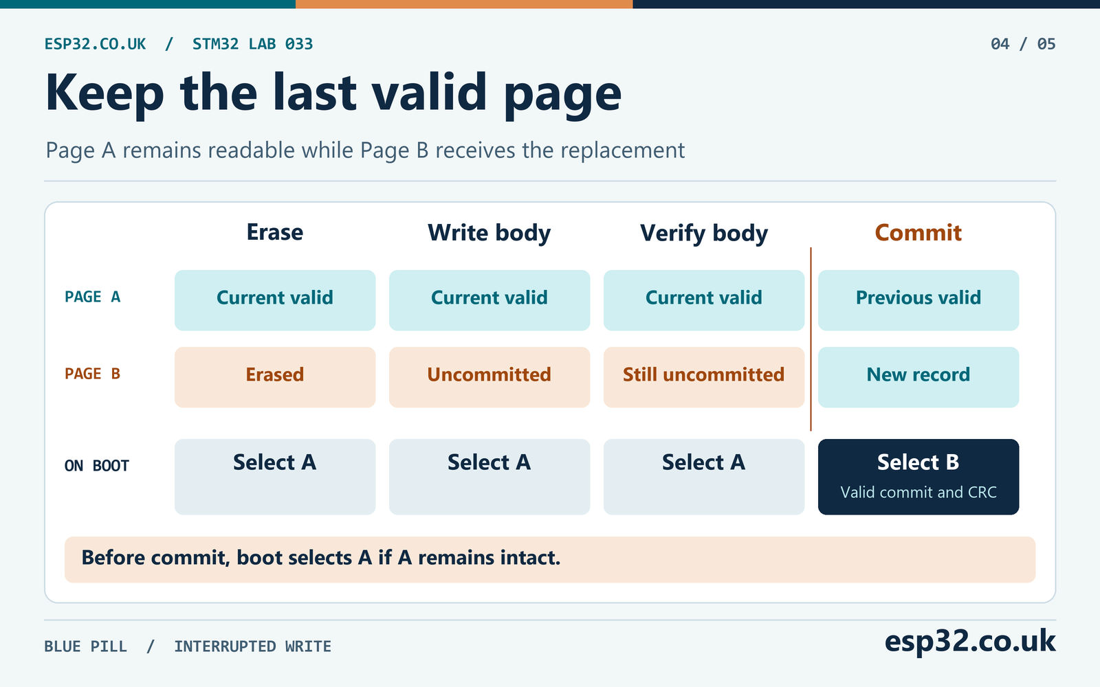
Suppose A is the newest valid record and the user requests a change. The module erases B, writes its body, reads the body back and finally programs its commit marker. A stays untouched throughout that sequence. After a successful write, both pages can be valid. The next load chooses B because it has the later sequence. The next changed save can then reuse A.
| When the operation stops | Page A | Page B | What the loader should select |
|---|---|---|---|
| Before B is erased | Current valid record | Empty or older record | A |
| After B is erased | Current valid record | Erased | A |
| During the B body write | Current valid record | Incomplete or uncommitted | A |
| After body readback, before commit | Current valid record | Complete body, erased commit | A |
| After a verified B commit | Previous valid record | Newest valid record | B |
An interruption during the commit itself can leave the marker erased, partial or fully programmed. The next boot uses the bytes it actually sees and accepts B only when every check succeeds. If the new record became valid just before a reset, it can be selected even if the application never reached the success return. That is why the durable record is authoritative after boot.
These recovery rules assume the interrupted operation affects the destination page and leaves the other page readable. They do not replace power supply design, a guaranteed write-energy budget or fault testing on the actual device. A marginal supply can create failures beyond the model. Plan settings writes for stable power and test repeated interruptions under the expected conditions.
For a controlled firmware test, temporarily build an early-return hook after the erase or before the commit, then reset and inspect which page loads. Keep the Flash lock step on the way out. That validates the logical recovery decision. It does not recreate a voltage collapse during an internal program pulse. For board-level fault testing, use a spare target and a controlled power setup, and inspect the Flash contents after each run.
Build a repeatable interruption test
First establish two known records. Keep one value obvious in A and another in B so the selected generation is visible on boot. Record the full contents of both pages. Test a save into the older slot, first with a normal build and then with a test hook placed at a single boundary. For each trial, reload the same known starting state through ordinary saves. This keeps a later test from accidentally using the result of the previous one as its starting point.
Useful hook positions are immediately after erase, halfway through the record body, after body readback and after the commit. At each position, have the test build end the attempt with the controller locked. Reset the existing firmware, then read both slots and record the boot result. Verify the selected sequence and both application values. This catches a loader that picks the correct-looking brightness while it accidentally takes the interval from the other page. The page that was active when the test started should remain byte-for-byte identical.
A second group can test validation failures using separate, deliberately constructed records on a spare target. For a CRC mismatch, write an altered body with the old CRC and a valid marker. For a range check, build a record with a correct CRC and an invalid setting. For a version check, use an unsupported version and compute the CRC over that body. This distinguishes rejection due to the intended check from rejection caused by an unrelated invalid field. Flash programming rules still apply to test data. Erase the target slot and write a complete test image through the programmer when making these deliberate fixtures.
For repeated power interruptions, use a test rig that can reproduce a measured cut and record its timing relative to the save. A spare GPIO set immediately before the foreground save can identify the start. A logic analyser trace alongside the supply waveform helps classify the outcome after restart. Log the starting sequence, requested values, cut time, both page dumps and loaded settings. The observable invariant is that, if the previously committed page remains intact, startup loads either that record or a complete verified replacement.
Budget Flash wear and write time
One changed save in this lab erases one page. The pages alternate, so 20,000 changed saves would produce roughly 10,000 erases per page. The datasheet lists 10 kcycles minimum endurance for the relevant suffix and temperature conditions, evaluated by characterisation. Treat the arithmetic as a planning illustration. Temperature, retention requirements and the part’s operating conditions determine the real design margin. ST DS5319, Flash characteristics and endurance
| Changed save rate | Time to 20,000 changed saves |
|---|---|
| 10 per day | 2,000 days, about 5.5 years |
| 1 per hour | About 833 days |
| 1 per minute | About 13.9 days |
Save explicit edits and skip unchanged values. A user dragging a brightness control can generate many intermediate positions. Apply those positions in RAM while the control is moving and save the final value after an idle period or a confirmation action. A data logger and a small configuration editor have different write patterns. Decide how often you can lose a recent change and design the commit policy around that requirement.
Erase also takes time. DS5319 lists up to 40 ms for a 1 KiB page erase and up to 70 µs per halfword program under the specified conditions. Nine programmed halfwords would add up to 0.63 ms of program time before readback, software and other overhead. Some slots skip halfwords that already match the erased state. Measure the operation on your target and budget it alongside peripheral deadlines.
On this Flash controller, access to main Flash during a program or erase can stall the CPU. Interrupt code fetched from Flash cannot be assumed to run on schedule during that interval. An independent watchdog can keep counting while the CPU waits. If you add persistent settings to the watchdog lab, measure the worst refresh gap around writes and compare it with the shortest watchdog deadline. STM32 IWDG and WWDG tutorial

Match the save window to the rest of the firmware
Check the deadlines of every function that shares the MCU. At 115,200 baud with eight data bits, no parity and one stop bit, each incoming byte uses ten wire bits. About 461 bytes can arrive in 40 ms. A simple interrupt-driven receiver may be unable to move data into a buffer while the core waits on a Flash access. With DMA, check how much autonomous transfer the design can sustain and how you will detect buffer wrap or overrun when execution resumes. Measure the actual receive path with sustained traffic during a changed save.
A save can be moved to an idle point in a command-response protocol. The host can send a complete update, wait for a durable reply and send its next command only after that reply. A stream with no flow control needs a different budget. Calculate the number of bytes arriving during the longest service gap, then account for current buffer occupancy, interrupt jitter and any delay after the write. Apply the same check to timer-driven sampling and CAN receive processing where dropped data matters.
Measure a changed save separately from an unchanged request. An unchanged request validates both slots and returns without erasing. Timing that path alone will miss the longest operation. Measure from just before the call through its final return and observe the supply during the write. Include this interval when sizing command timeouts and reviewing watchdog margins. Use the datasheet operating limits for the intended MCU suffix and conditions when evaluating those margins.
Preserve settings across firmware updates
Treat the reservation as part of the firmware’s published memory layout. Every firmware that can be installed on the same board needs to agree on which bytes it owns. Keep the 62 KiB application limit in all build profiles, including recovery builds used during service. If a bootloader is added later, re-evaluate its own Flash range and the offset application range together, and keep the two settings pages outside both writable images.
Inspect the output your updater actually reads. An ELF or Intel HEX file conveys addresses. A raw binary needs a separately configured base address and a known byte length. A 62 KiB limit on the linker region helps keep the build inside its range, and a check on the delivered update file catches packaging steps that pad or merge it. Use the updater’s write and erase plan to confirm the last application byte is at or below 0x0800F7FF. With page granularity the last application page starts at 0x0800F400.
Use a small upgrade acceptance test. Install the original build on a spare board, save known values twice and capture both settings pages. Update with the same tool, options and artifact type used in service. Compare the saved pages after programming and confirm the new firmware loads the expected sequence and values. Repeat with the newest record in the other page so the test covers both possible selections. If a downgrade is supported, run it as a separate case with a format that the older firmware can read.
Changing the fields or their interpretation needs a migration policy. With two valid versions, decide which image can read each one and when the older slot may be reclaimed. If an older build accepts only version 1, it may load the last version 1 snapshot after a rollback while a newer build can see the more recent version 2 snapshot. Decide whether that rollback behaviour is acceptable before shipping the migration. A product that must preserve every updated setting across downgrade needs a compatible shared representation or a migration plan with its own retained copy.
Diagnose Flash settings failures
| Symptom | First check | Likely cause |
|---|---|---|
| Linker says Flash overflow | Active script and map | Code plus Flash load data exceeds 62 KiB |
| Bad layout result | Linker symbols and reported capacity | Wrong part, linker script or application offset |
| Flash error before commit | HAL error code, page address and protection | Erase or program failed |
| Empty result after an update | Dump both pages | Programmer erased the settings region or version changed |
| One record is skipped | Marker, CRC and ranges | Interrupted or invalid record |
| Save seems to disturb serial traffic | Measure the erase interval | Flash access stalls the main loop or interrupt code |
| Settings reset during a test | Check for a reflash or mass erase | Programming tool touched the reservation |
When diagnosing a write error, record HAL_FLASH_GetError() after the failing call while the information is still current. Confirm that the target address is the expected page and that it is writable. Avoid removing Flash protection as a first diagnostic step. Determine why that protection exists and whether your application is meant to own the page.
For a read problem, inspect the data as 16-bit halfwords and then as bytes. Check that the sequence and CRC halves appear in the documented order. If the record looks complete but the firmware rejects it, calculate the CRC over exactly the first 12 bytes and check the setting ranges. Changing the record version, byte order or covered fields requires updating the reader and writer together.
Check the reset source when a save appears to reboot the board. A watchdog reset, supply dip and a fault from a misaddressed write can look similar from the application UI. Read the reset flags and retain the conditions that produced the failure. A short test with no peripherals is a useful baseline before you combine storage with CAN, serial reception or timed sampling.
Questions about STM32 Flash settings
Can I use the same final-page addresses on a Black Pill?
Recalculate the reservation using the actual MCU’s capacity, erase geometry, program width and linker script. The two addresses here belong to a 64 KiB STM32F103C8 layout. A different STM32 family can use sectors, different write widths or additional cache requirements.
Does a reset erase the stored values?
A normal reset leaves the Flash cells intact. A programmer erase, firmware update or application write can change them. Test the exact update procedure and the exact boot path that will run on the deployed device.
Should a boot with no valid record immediately write the defaults?
The lab loads defaults in RAM and waits for an explicit save. That keeps boot independent of Flash writes and avoids consuming a cycle on a transient read or migration problem. An application that needs a factory record can provision it through a separate, deliberate step.
Can I save every sensor reading?
Estimate your save rate against erase endurance and acceptable data loss. The one-record-per-page lab suits occasional configuration changes. Frequent logging typically needs batching, an append-style design or storage selected for the expected write workload.