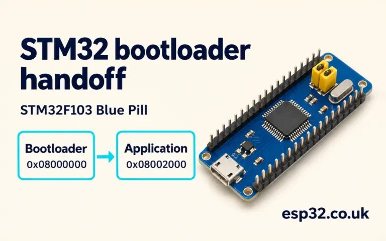
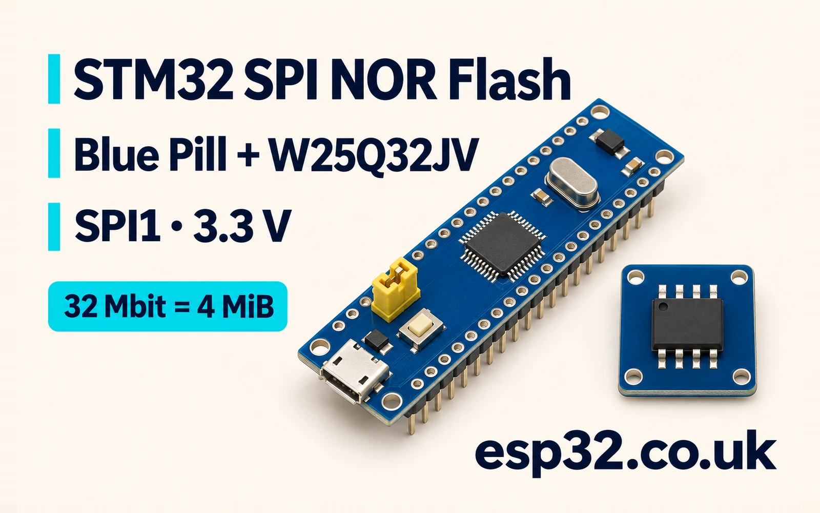
This esp32PriceAliExpress price.co.uk/ guide connects a Winbond W25Q32JV serial NOR Flash chip to an STM32F103 Blue PillPriceAliExpress price. The lab reads the JEDEC ID, erases a single 4 KiB scratch sector and programs a 32-byte pattern that crosses a page boundary. A final read compares every byte. The same command sequence works as a starting point for fixed resources, configuration records or a small raw log.
Use SPI1 on PA5, PA6 and PA7, with PA4 as an active-low chip select. Run the chip at 3.3 V and use SPI mode 0 for the lab. The W25Q32JV holds 32 Mbit, which is 4 MiB of addressable bytes. Its Page Program instruction stays inside a 256-byte page and its smallest erase unit is a 4 KiB sector. Keep these two sizes separate when deciding how to update an address.
What external SPI NOR adds to a Blue Pill
The STM32PriceAliExpress price’s internal Flash contains its firmware and is mapped into the processor’s address space. The external device in this lab sits on a serial bus. To read it, the MCU sends an opcode and an address, then supplies clock pulses so the chip can shift data back. The standard SPI1 interface on this STM32F103 does not make the external chip directly addressable by an ordinary pointer. Read bytes into RAM before parsing them or passing them to an application.
Serial NOR gives you explicit byte addresses, page programs and sector erases. A microSD card presents a different interface through its own controller and typically carries a filesystem. Decide which abstraction you need before designing the update procedure. A flat NOR address space makes offsets predictable, while erases, lifetime and power-loss recovery are responsibilities of the storage layout. Blue Pill internal Flash settings lab · STM32 SPI microSD and FatFs lab
The target part is the 3 V W25Q32JV in an 8-pin package with the ordering suffix IQ, such as W25Q32JVSSIQ. The example accepts the JEDEC bytes EF 40 16. Read the chip marking and match it against the order table. A breakout sold under a short family name can carry a different density, supply class or command set. A matching ID helps confirm the connection and geometry for the selected part. Several older Winbond parts can share that ID, so the printed part number and its datasheet remain relevant. Winbond W25Q32JV datasheet
| Property | W25Q32JV lab value |
|---|---|
| Capacity | 32 Mbit = 4,194,304 bytes = 4 MiB |
| Address bytes on the SPI wire | Three, most significant first |
| Valid byte addresses | 0x000000 to 0x3FFFFF inclusive |
| Page size | 256 bytes |
| Smallest erase size | 4,096 bytes |
| Pages per sector | 16 |
| Sectors per device | 1,024 |
| Erased data | 0xFF at each byte |
Wire the W25Q32JV to SPI1
Use a bare chip on a suitable breakout or a module whose pinout and voltage are known. Wire it with the board powered down. The table uses the standard 8-pin SOIC connections for the specified lab part. Check the orientation mark before attaching a bare package. Breakout connector order can differ from IC pin order, even when the board labels use the same names.
| STM32 or rail | Flash signal | SOIC-8 pin | Purpose |
|---|---|---|---|
| PA4, GPIO output | /CS | 1 | Select the Flash while low |
| PA6, SPI1_MISO | DO / IO1 | 2 | Data from Flash to MCU |
| 3.3 V | /WP / IO2 | 3 | Hold high for single SPI |
| GND | GND | 4 | Common reference |
| PA7, SPI1_MOSI | DI / IO0 | 5 | Commands, addresses and data from MCU |
| PA5, SPI1_SCK | CLK | 6 | SPI clock |
| 3.3 V | /HOLD or /RESET / IO3 | 7 | Hold high for single SPI |
| 3.3 V | VCC | 8 | Supply |
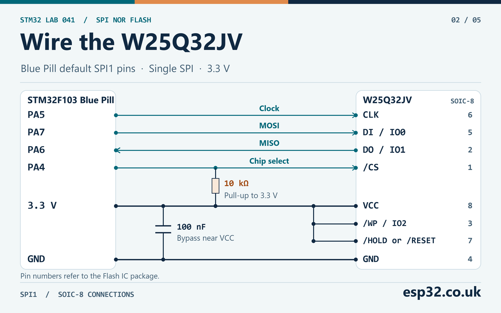
Fit a 100 nF ceramic capacitor across VCC and GND near the Flash. An external pull-up such as 10 kΩ from /CS to 3.3 V keeps the chip deselected before the STM32 configures PA4. Also initialise the GPIO output level high. On a module, inspect any regulators, pull-ups or level shifters before adding more components. The chosen JV part operates on a 3.3 V rail. The fact that a GPIO pin on the STM32 tolerates a higher input voltage says nothing about the Flash supply or inputs. STM32F103C8 datasheet · Blue Pill pinout
In this lab the extra I/O pins remain high. The device also supports dual and quad transfers, and the meaning of those pins changes in those modes. A breakout may label them IO2 and IO3 regardless of how you use it. Check the suffix-specific pin table if a different board brings out a reset function on pin 7. Keep the clock wire short, give it a nearby ground return and attach the logic analyser ground to the same reference.
Configure STM32CubeMX and check the SPI clock
Select the STM32F103C8 and keep Serial Wire debugging enabled. Enable SPI1 in full-duplex master mode with the default pin mapping. Configure PA4 separately as GPIO output, push-pull, initial level high. For the default mapping, PA5 and PA7 are alternate-function outputs and PA6 is a peripheral input. Keep any other device on the same bus deselected during the initial test. CubeMX and CubeIDE setup · STM32 SPI and HAL guide
| SPI1 setting | Lab value |
|---|---|
| Mode | Master, full-duplex, two lines |
| Data size | 8 bits |
| First bit | MSB |
| Clock polarity | Low |
| Clock phase | First edge |
| NSS | Software |
| SPI CRC and TI mode | Disabled |
| Divider with nominal 8 MHz PCLK2 | 8 for approximately 1 MHz SCK |
SPI1 runs from APB2. With nominal 8 MHz HSI and no APB2 division, 8 MHz ÷ 8 = 1 MHz. If you instead configure a 72 MHz PCLK2, a divider of 64 gives 1.125 MHz and a divider of 128 gives 562.5 kHz. Choose a slow initial rate and measure it. Mode 0 has idle-low SCK, with data sampled on rising edges. The Flash also supports mode 3, but the driver below deliberately checks mode 0. ST RM0008 reference manual
GPIO chip select lets one assertion cover the complete command. Hold it low through all command, address and data clocks for that transaction. The code can make multiple HAL calls while PA4 stays low. This is how the driver sends a header and then reads a variable-length result without an intermediate deselect. In the audited CubeF1 source, the blocking transmit and transmit/receive calls handle the transaction-end peripheral checks before a successful return. The software then releases the pin. ST CubeF1 SPI HAL v1.1.10
Hardware SPI CRC would insert traffic that the Flash command protocol does not call for. Keep it disabled. If a stored record needs a CRC, calculate it over the application’s record bytes and store the result as part of the record format. ES096 describes F1 SPI CRC limitations in certain configurations. The simple lab uses polling in master mode and keeps that peripheral feature disabled. ST ES096 device errata · STM32 hardware CRC32 guide
Start with a read-only JEDEC ID
Let the Flash supply settle and keep chip select high during power-up. The Winbond power-up specification includes a read-access interval and a separate write-inhibit interval. The driver waits 20 ms after it drives /CS high. This assumes the Flash is already powered from the stable board rail. A Flash supply switched later in firmware needs its own wait measured from that supply’s rise.
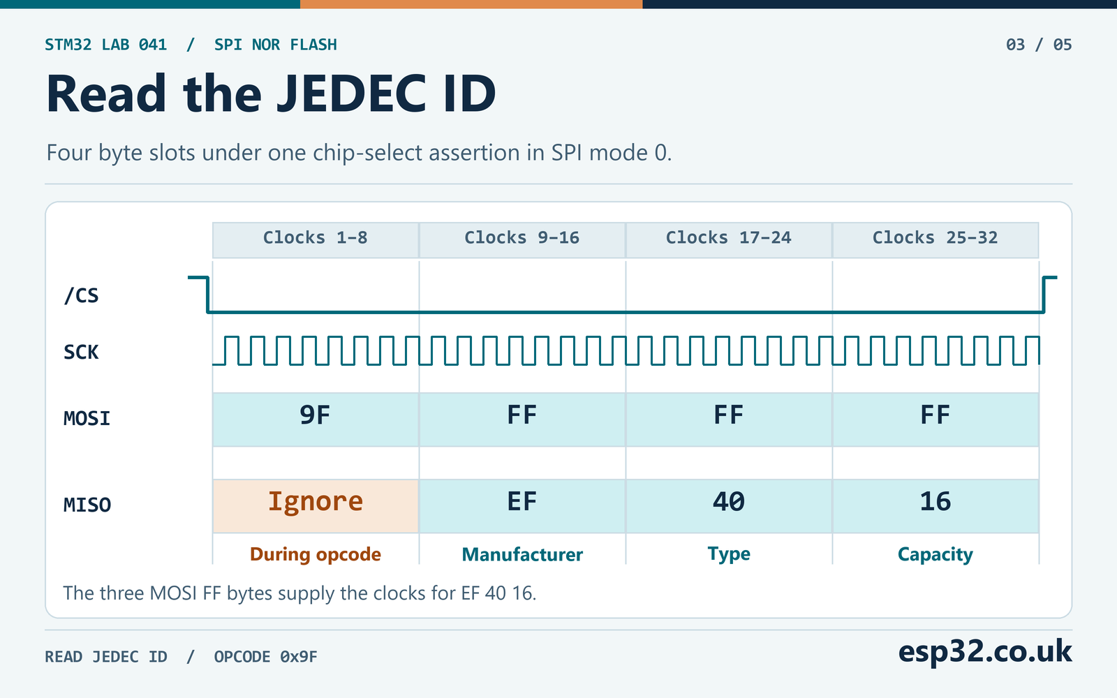
Send opcode 0x9F and then clock three more bytes with chip select held low. In the lab the MOSI trace is 9F FF FF FF. The last three transmitted bytes merely supply clocks. Ignore the MISO byte during the opcode. The next three bytes should be EF 40 16. EF is Winbond’s manufacturer code, 40 is the expected memory-type byte and 16 is the capacity code for this version. Inspect the four byte windows together on the analyser. If all four are taken as returned ID bytes, the result appears shifted even when the wire traffic is correct.
An MCU reset does not necessarily reset the external Flash. If the STM32 resets during an erase, the chip can remain busy until that operation finishes, assuming its rail stayed up. If previous firmware put the part into deep power-down, a fresh MCU reset may leave it asleep. For this lab start from a cold, known setup. If the ID fails after a reset, wait for the previous operation to finish and probe again. Follow the exact device’s wake-up timing if you add a low-power state.
Winbond also documents variants with device bytes 70 16. This driver stops on those bytes because it deliberately accepts the selected EF 40 16 variant. A different result that looks coherent is a reason to identify the actual part and confirm its datasheet. A result of all ones often means DO is undriven or pulled high. All zeros can result from DO held low. Neither pattern diagnoses the fault on its own. Check power, continuity, the CS waveform and whether the Flash actually drives its output during the three return bytes.
Follow the command and status sequence
The status register has two bits you need for a basic write. Bit 0 is BUSY, often called WIP or write in progress. Bit 1 is the write-enable latch, WEL. A power-up or a completed program or erase clears WEL. Before each operation that changes the array, send Write Enable as its own transaction. End that transaction by bringing chip select high. Then read the status and verify WEL before issuing a program or erase.
| Opcode | Transaction while selected | Use |
|---|---|---|
9F | Opcode, then three read bytes | Read JEDEC ID |
05 | Opcode, then at least one read byte | Read Status Register 1 |
06 | Opcode only | Set WEL |
04 | Opcode only | Clear WEL |
03 | Opcode, three address bytes, then data read clocks | Read array data |
02 | Opcode, three address bytes, then program bytes | Program part or all of one page |
20 | Opcode and three address bytes | Erase one 4 KiB sector |
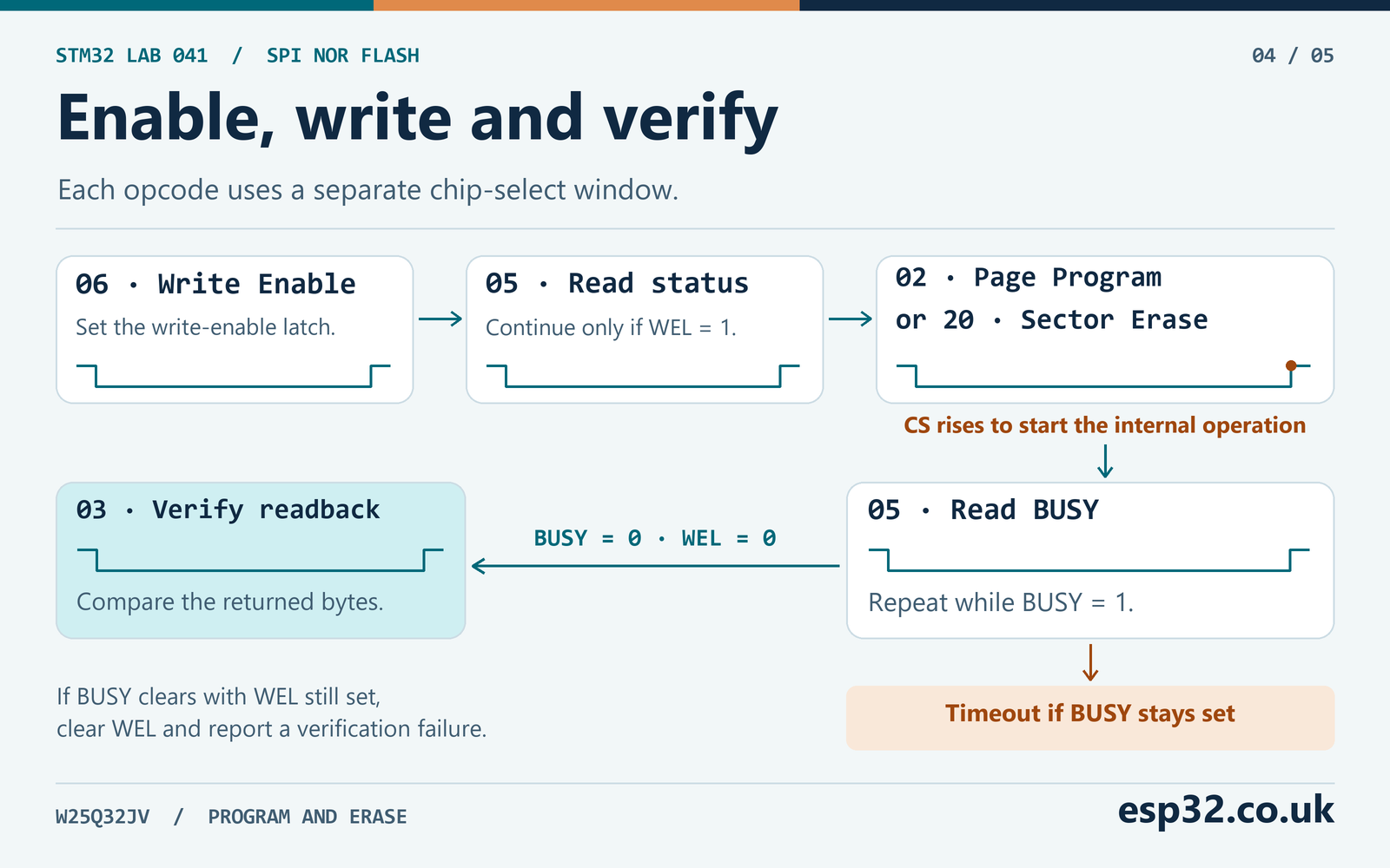
For example, erasing the lab sector produces 06, a status read 05 FF, and then 20 00 30 00, each with its own chip-select window. The erase starts when chip select rises after the full command. Read Status Register 1 in later windows and poll until BUSY is clear. A fast operation may finish before the first poll sees BUSY asserted. A driver that requires seeing BUSY go high can reject a successful short operation.
The lab budgets 20 ms for the program polling loop and 600 ms for the erase polling loop. The Winbond data sheet lists maximum internal times of 3 ms for Page Program and 400 ms for Sector Erase under its specified operating conditions. The software budgets leave room for polling overhead. They exclude the later verification read and are separate from the HAL timeout used for individual SPI transfers. Keep the HAL tick running during the call. The polling loop uses unsigned elapsed time so it can cross a millisecond tick rollover.
If BUSY is clear and WEL is still high after the command, the code attempts Write Disable and reports a verification failure. That combination is useful evidence that the command did not complete in the expected way. It does not tell you why. If the SPI transfer fails or the polling budget expires, the code exits with chip select high. The device may still be busy or may have accepted part of the attempted program. Read status and inspect the affected region before choosing how to recover.
Protection is separate from the basic WEL check. The Winbond device can protect ranges through status register settings or individual block and sector locks. The /WP pin also participates in status-register protection in applicable modes. Driving it high keeps the pin inactive for the bench connection. It does not clear protection stored inside the chip. Read the part’s status and lock configuration if writes fail while reads work. The lab leaves those settings untouched.
Calculate the sector and page boundaries
An erased NOR byte reads as FF, with all eight bits set. Programming can clear bits to zero. To set a cleared bit back to one, erase the sector that contains it. A byte of F0 has four low bits already cleared, so it cannot be turned into FF by programming FF. The driver takes a conservative approach and checks that each target byte is FF before it sends Page Program. It does not reprogram bytes that already contain data.
The scratch sector starts at 0x003000 and ends at 0x003FFF. The driver requires a sector-aligned starting address for an erase. This forces the caller to name the whole affected range. Passing an address inside a sector and silently rounding it down can erase data the caller expected to preserve. Verify the full sector reads as FF after erasing. A byte elsewhere in that sector belongs to the same erase unit, even if you only intend to write a small record.
The 32-byte sample starts at 0x0030F0. A page offset is the address modulo 256, so this address is at offset 0xF0, or 240. That leaves 256 − 240 = 16 bytes before the page ends. Program the first 16 bytes at 0x0030F0, then start a new write-enable and program sequence for the remaining 16 bytes at 0x003100.
| Stage | Byte address or range | Value |
|---|---|---|
| Erase | 0x003000–0x003FFF | One 4 KiB sector |
| Program first page | 0x0030F0–0x0030FF | A0 through AF |
| Program second page | 0x003100–0x00310F | B0 through BF |
| Read and compare | 0x0030F0–0x00310F | All 32 bytes in order |
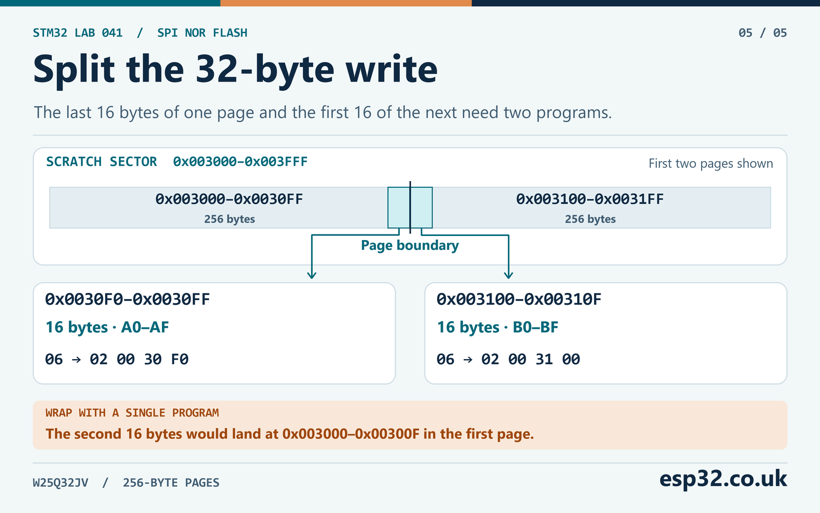
A single 32-byte Page Program starting at 0x0030F0 would wrap inside the original page. Its second group of 16 bytes would land at the beginning of that page, from 0x003000 to 0x00300F. The command would never reach the next page. This is why the page boundary check happens before Write Enable. The standard 03 read can cross page boundaries. A continuous read from 0x0030F0 can therefore recover the 32-byte result in one transaction.
For a general buffer, calculate the bytes left in the current page as 256 - (address % 256). Program the smaller of that value and the remaining length. Advance the source pointer and address by the number written, then repeat. Validate the whole intended span against the chip size before starting the first write. A later range error would otherwise leave the earlier pages changed. An aligned full page uses a single operation, while an unaligned range can need an extra one.
Address bytes travel most significant first. The read header for the sample is 03 00 30 F0, followed by 32 clocked bytes. The two program headers are 02 00 30 F0 and 02 00 31 00. Write those expected byte strings beside the trace when debugging. Copying the low three bytes of a native little-endian integer to SPI would reverse the address bytes. The driver constructs the header explicitly and rejects a span beyond 0x3FFFFF, including a two-byte read starting at the final address.
The first data byte of a standard 03 read is available immediately after the three address bytes. On the logic analyser, the first FF transmitted after the address should line up with the first returned data byte. These filler bytes supply the clock for the receive phase. They are distinct from an extra dummy phase specified by some fast-read commands. Adding an extra byte between the address and the returned data for this opcode would discard the first real byte. Conversely, switching to a fast-read opcode requires following that opcode’s own timing diagram.
Add the HAL driver
Place w25q32_lab.h in the project include path and add w25q32_lab.c to the build. The module expects PA4 chip select and the SPI1 settings in the table. Use a zero-initialised NorFlash and open it before accessing the array. The open call fills the ID buffer when the transfer succeeds, even when the ID is unexpected. It only enables the other API calls after the expected ID matches.
#ifndef W25Q32_LAB_H
#define W25Q32_LAB_H

#include "stm32f1xx_hal.h"

enum {
    NOR_CAPACITY = 0x400000, NOR_PAGE_SIZE = 256, NOR_SECTOR_SIZE = 4096
};

typedef struct { SPI_HandleTypeDef *spi; } NorFlash;
typedef enum {
    NOR_OK, NOR_ARG, NOR_ID, NOR_SPI, NOR_BUSY, NOR_WEL,
    NOR_TIMEOUT, NOR_NOT_ERASED, NOR_VERIFY
} NorResult;

NorResult Nor_Open(NorFlash *flash, SPI_HandleTypeDef *spi, uint8_t id[3]);
NorResult Nor_Read(NorFlash *flash, uint32_t addr, uint8_t *data, uint16_t length);
NorResult Nor_ProgramPage(NorFlash *flash, uint32_t addr, const uint8_t *data, uint16_t length);
NorResult Nor_EraseSector(NorFlash *flash, uint32_t addr);

#endif
#include "w25q32_lab.h"
#include <string.h>
enum { WIP = 1, WEL = 2, SPI_MS = 25, PROGRAM_MS = 20, ERASE_MS = 600, CHUNK = 64 };
static NorResult transfer(SPI_HandleTypeDef *spi, const uint8_t *cmd, uint16_t header,
const uint8_t *out, uint8_t *in, uint16_t count)
{
HAL_GPIO_WritePin(GPIOA, GPIO_PIN_4, GPIO_PIN_RESET);
HAL_StatusTypeDef status = HAL_SPI_Transmit(spi, cmd, header, SPI_MS);
if (status == HAL_OK && out != NULL) {
status = HAL_SPI_Transmit(spi, out, count, SPI_MS);
}
if (status == HAL_OK && in != NULL) {
uint8_t dummy[CHUNK];
memset(dummy, 0xFF, sizeof dummy);
while (count != 0U && status == HAL_OK) {
uint16_t n = count > CHUNK ? CHUNK : count;
status = HAL_SPI_TransmitReceive(spi, dummy, in, n, SPI_MS);
count = (uint16_t)(count - n);
in += n;
}
}
HAL_GPIO_WritePin(GPIOA, GPIO_PIN_4, GPIO_PIN_SET);
return status == HAL_OK ? NOR_OK : NOR_SPI;
}
static NorResult simple(SPI_HandleTypeDef *spi, uint8_t cmd)
{
return transfer(spi, &cmd, 1, NULL, NULL, 0);
}
static NorResult status1(SPI_HandleTypeDef *spi, uint8_t *status)
{
const uint8_t cmd = 0x05;
return transfer(spi, &cmd, 1, NULL, status, 1);
}
static NorResult idle(SPI_HandleTypeDef *spi)
{
uint8_t status;
NorResult result = status1(spi, &status);
if (result != NOR_OK) {
return result;
}
return (status & WIP) ? NOR_BUSY : NOR_OK;
}
static NorResult enable_write(SPI_HandleTypeDef *spi)
{
NorResult result = simple(spi, 0x06);
uint8_t status = 0;
if (result == NOR_OK) {
result = status1(spi, &status);
}
if (result != NOR_OK) {
return result;
}
return (status & (WIP | WEL)) == WEL ? NOR_OK : NOR_WEL;
}
static NorResult finish_write(SPI_HandleTypeDef *spi, uint32_t budget)
{
uint32_t start = HAL_GetTick();
do {
uint8_t status;
NorResult result = status1(spi, &status);
if (result != NOR_OK) {
return result;
}
if (!(status & WIP)) {
if (!(status & WEL)) {
return NOR_OK;
}
result = simple(spi, 0x04);
return result == NOR_OK ? NOR_VERIFY : result;
}
HAL_Delay(1);
} while ((uint32_t)(HAL_GetTick() - start) < budget);
return NOR_TIMEOUT;
}
static NorResult addressed(SPI_HandleTypeDef *spi, uint8_t opcode, uint32_t addr,
const uint8_t *out, uint8_t *in, uint16_t count)
{
uint8_t cmd[] = {opcode, (uint8_t)(addr >> 16), (uint8_t)(addr >> 8), (uint8_t)addr};
return transfer(spi, cmd, sizeof cmd, out, in, count);
}
static NorResult compare(SPI_HandleTypeDef *spi, uint32_t addr,
const uint8_t *expected, uint16_t length)
{
uint8_t sample[CHUNK];
for (uint16_t offset = 0; offset < length;) {
uint16_t left = (uint16_t)(length - offset);
uint16_t n = left > CHUNK ? CHUNK : left;
NorResult result = addressed(spi, 0x03, addr + offset, NULL, sample, n);
if (result != NOR_OK) {
return result;
}
for (uint16_t i = 0; i < n; ++i) {
uint8_t wanted = expected ? expected[offset + i] : 0xFFU;
if (sample[i] != wanted) {
return NOR_VERIFY;
}
}
offset = (uint16_t)(offset + n);
}
return NOR_OK;
}
static int in_range(NorFlash *flash, uint32_t addr, uint16_t length)
{
return flash && flash->spi && length != 0U && addr < NOR_CAPACITY &&
length <= NOR_CAPACITY - addr;
}
NorResult Nor_Open(NorFlash *flash, SPI_HandleTypeDef *spi, uint8_t id[3])
{
if (flash == NULL) {
return NOR_ARG;
}
flash->spi = NULL;
if (!spi || !id || spi->Instance != SPI1 || spi->Init.Mode != SPI_MODE_MASTER ||
spi->Init.Direction != SPI_DIRECTION_2LINES || spi->Init.DataSize != SPI_DATASIZE_8BIT ||
spi->Init.CLKPolarity != SPI_POLARITY_LOW || spi->Init.CLKPhase != SPI_PHASE_1EDGE ||
spi->Init.NSS != SPI_NSS_SOFT || spi->Init.FirstBit != SPI_FIRSTBIT_MSB ||
spi->Init.CRCCalculation != SPI_CRCCALCULATION_DISABLE) {
return NOR_ARG;
}
HAL_GPIO_WritePin(GPIOA, GPIO_PIN_4, GPIO_PIN_SET);
HAL_Delay(20);
const uint8_t cmd = 0x9F;
NorResult result = transfer(spi, &cmd, 1, NULL, id, 3);
if (result != NOR_OK) {
return result;
}
if (id[0] != 0xEFU || id[1] != 0x40U || id[2] != 0x16U) {
return NOR_ID;
}
flash->spi = spi;
return NOR_OK;
}
NorResult Nor_Read(NorFlash *flash, uint32_t addr, uint8_t *data, uint16_t length)
{
if (!data || !in_range(flash, addr, length)) {
return NOR_ARG;
}
NorResult result = idle(flash->spi);
if (result != NOR_OK) {
return result;
}
return addressed(flash->spi, 0x03, addr, NULL, data, length);
}
NorResult Nor_ProgramPage(NorFlash *flash, uint32_t addr, const uint8_t *data, uint16_t length)
{
if (!data || !in_range(flash, addr, length) ||
length > NOR_PAGE_SIZE - (addr % NOR_PAGE_SIZE)) {
return NOR_ARG;
}
NorResult result = idle(flash->spi);
if (result == NOR_OK) {
result = compare(flash->spi, addr, NULL, length);
if (result == NOR_VERIFY) {
return NOR_NOT_ERASED;
}
}
if (result == NOR_OK) {
result = enable_write(flash->spi);
}
if (result == NOR_OK) {
result = addressed(flash->spi, 0x02, addr, data, NULL, length);
}
if (result == NOR_OK) {
result = finish_write(flash->spi, PROGRAM_MS);
}
return result == NOR_OK ? compare(flash->spi, addr, data, length) : result;
}
NorResult Nor_EraseSector(NorFlash *flash, uint32_t addr)
{
if ((addr % NOR_SECTOR_SIZE) != 0U || !in_range(flash, addr, NOR_SECTOR_SIZE)) {
return NOR_ARG;
}
NorResult result = idle(flash->spi);
if (result == NOR_OK) {
result = enable_write(flash->spi);
}
if (result == NOR_OK) {
result = addressed(flash->spi, 0x20, addr, NULL, NULL, 0);
}
if (result == NOR_OK) {
result = finish_write(flash->spi, ERASE_MS);
}
return result == NOR_OK ? compare(flash->spi, addr, NULL, NOR_SECTOR_SIZE) : result;
}The driver uses a single foreground caller. The separate HAL calls inside a chip-select window are one device transaction and must not be interleaved with work for another SPI client. On a shared bus, protect the window with the same ownership mechanism used by the other clients. Also serialise the logical WREN, write and verification sequence for each Flash chip. A bus mutex held only while one HAL call is active would leave the command header, data and chip-select state exposed to interleaving.
The API takes a uint16_t read length. For a large dump, read successive bounded chunks with explicit addresses and verify the overall span in the caller. The driver generates the read clocks using a small fixed buffer of FF bytes and receives into the caller’s destination. It can refill the data in several HAL calls without releasing chip select. For verification it uses addressed reads in small blocks, which keeps the stack requirement modest even when checking an entire sector.
Run the scratch-sector test once
Use a part reserved for the lab, or confirm that every byte of 0x003000–0x003FFF may be erased. On a chip from an existing product, read and preserve any data you need first. The test below separates the read-only probe from the erase. The global nor_run starts at zero. Once the debugger shows the expected ID and you have checked the scratch range, set it to one to run the write sequence. The application then stops issuing Flash commands.
Put the include and watch declarations at file scope. Insert the rest in the main function after the generated GPIO and SPI initialisation. Keep the generated clock and SysTick setup. The local arrays passed to the driver are ordinary C buffers. The volatile copies are only for displaying the results in the debugger.
/* File scope */
#include "w25q32_lab.h"
#include <string.h>
volatile NorResult nor_result;
volatile uint8_t nor_run;
volatile uint8_t nor_id_watch[3], nor_watch[32];

/* After MX_GPIO_Init() and MX_SPI1_Init() */
NorFlash flash = {0};
uint8_t id[3] = {0};
nor_result = Nor_Open(&flash, &hspi1, id);
for (unsigned i = 0; i < 3; ++i) {
    nor_id_watch[i] = id[i];
}
while (!nor_run) {}

if (nor_result == NOR_OK) {
    uint8_t tx[32], rx[32];
    for (unsigned i = 0; i < sizeof tx; ++i) {
        tx[i] = (uint8_t)(0xA0U + i);
    }
    nor_result = Nor_EraseSector(&flash, 0x003000U);
    if (nor_result == NOR_OK)
        nor_result = Nor_ProgramPage(&flash, 0x0030F0U, tx, 16);
    if (nor_result == NOR_OK)
        nor_result = Nor_ProgramPage(&flash, 0x003100U, tx + 16, 16);
    if (nor_result == NOR_OK)
        nor_result = Nor_Read(&flash, 0x0030F0U, rx, sizeof rx);
    if (nor_result == NOR_OK) {
        for (unsigned i = 0; i < sizeof rx; ++i) {
            nor_watch[i] = rx[i];
        }
        if (memcmp(tx, rx, sizeof tx) != 0)
            nor_result = NOR_VERIFY;
    }
}
for (;;) {}
Program over SWD and let the MCU reach the wait on nor_run. Check the ID before enabling the test. After the operations finish, the watch should show NOR_OK, with the first byte A0, byte 15 AF, byte 16 B0 and byte 31 BF. The numeric indices here are zero based. If you want to prove persistence, reset and run only the open and read paths. Keep the erase disabled and verify the same 32 bytes before attempting another write. STM32 SWD flashing guide
A useful negative test is to pass length 32 to Nor_ProgramPage() at 0x0030F0. The function should return NOR_ARG before any transaction. After a successful first run, try programming the same first 16 bytes again without erasing. The expected result is NOR_NOT_ERASED, and a trace should show only the status check and read preflight. Those tests exercise both guards without issuing an invalid program to the device.
To verify the boundary on a fresh scratch sector, also read a few bytes at the beginning of the first page and immediately after the end of the pattern. They should still read as FF in the lab. If you deliberately filled a neighbouring sector before the test, compare that data too. The program readback in the module checks the requested bytes. Checking surrounding locations in this separate experiment helps catch an incorrect address or an unexpected wrap that affects bytes outside the requested span. Record the initial state before testing, since bytes from a previous run can otherwise resemble a new failure.
Estimate the bus and array time separately
At 1 MHz one byte takes 8 µs on the wire. The four-byte read header and 32 data bytes require 36 bytes of clocking, or 288 µs before software overhead. Each half of the split program sends a four-byte header and 16 data bytes, so it occupies 160 µs of clocks. A full-page program would clock 260 bytes in 2.080 ms at the same bus rate. Each write also takes internal time after chip select rises. Increasing SCK reduces the transfer time and leaves the internal program and erase times in place.
The sector verification checks 64 chunks of 64 bytes. It clocks 4,096 data bytes and 256 command and address bytes. At 1 MHz that is about 34.816 ms of wire time, plus the gaps between transfers. A raw continuous sector read could carry all 4,096 bytes after just one header. The verification loop trades extra headers for a small buffer and bounded calls. Include the readback cost when estimating how often a blocking task can run.
If you integrate this into a logger, size the input queue for the worst measured pause rather than the typical program time. An erase can dominate the schedule. For example, collecting 500 bytes/s during a 400 ms erase plus approximately 35 ms of verification accumulates about 218 bytes, before scheduler and transfer overhead. Pre-erased sectors can shift the erase work to a planned idle period. Keep a counter for dropped records if the producer can overrun its queue.
Troubleshoot from the first failing transaction
Begin with a short logic-analyser capture of chip select, CLK, DI and DO. Trigger on chip select falling. Set the SPI decoder to mode 0, MSB first and eight bits. Check the four bytes of the ID exchange before checking the longer write sequence. Then look at the status register after 06 and verify that chip select actually rose between Write Enable and the next opcode. A correct waveform in one window cannot compensate for a missing boundary between windows.
| Symptom | Check first |
|---|---|
ID is FF FF FF | VCC, chip select, DO continuity, power-down state and whether the device is busy |
ID is 00 00 00 | A shorted or held-low DO line, orientation and power |
| ID is stable but differs | Part marking, suffix and decoder alignment |
NOR_ARG before any clocks | SPI setup, probe result, range, alignment and page room |
NOR_WEL | Separate 06 window, power-up delay and the status byte |
NOR_BUSY | A prior operation still running or incorrect status read |
NOR_TIMEOUT | Status bus integrity, supply stability and HAL tick |
NOR_NOT_ERASED | Verify the target bytes and the intended sector |
NOR_VERIFY | Status protection, address order, contents and command boundaries |
NOR_SPI | HAL error, peripheral state, clocks and ownership of SPI1 |
If the ID reads correctly but data repeat every 256 bytes, check the address construction and the analyser’s byte boundaries. If only the first part of a page write is present at the intended address, inspect the beginning of that same page for wraparound. An incorrect address byte can also put a good pattern in the wrong sector. Compare the command address to the expected trace before issuing any additional erase.
If readback is wrong after a transfer error, wait for BUSY to clear before testing the contents. A partially sent page command can still alter some bytes when the controller raises chip select. There is no safe automatic retry that reconstructs unknown prior data. Decide whether the area is disposable or recoverable from a backup. For a disposable scratch sector you can erase it again and verify it before rebuilding the pattern.
If the status read returns FF while the bus is supposed to be idle, the BUSY bit will also appear set. A disconnected DO line can therefore resemble a busy chip to the polling loop. Correlate the status with a new ID probe and with the waveform. A chip that really is busy may decline the ID command until the current operation ends. When a complete power cycle is appropriate for the disposable test part, capture the first ID and status after the power-up delay before trying any write. This helps separate a bad return line from a failing program sequence.
Readback through the same SPI path can also share a systematic wiring or decoding error. A repeatable result at a very slow clock followed by failures at a higher clock points toward timing or signal integrity. Check the signal at the Flash pins, shorten the clock and data wires and compare the same operation at both rates. A logic analyser tells you how it decoded the thresholds. A scope can show edge shape and ringing between those thresholds.
Choose an update layout before storing real data
A record can hold a version, length, sequence number, payload and checksum. The read path can verify those fields before trusting the payload. Keep record byte order explicit, particularly if tools on a PC will read the same dump. Keep an address map that names the occupied sectors and the ranges reserved for firmware, assets or calibration. A small format with known bounds is easier to inspect than a raw C structure whose padding depends on the compiler.
If an existing record must survive an interrupted update, keep a valid copy in a different erase sector while writing the new one. Write into an erased range, read it back, and design a commit rule so boot code can distinguish a complete record from a partially written one. For this driver, a separate commit field must start in erased bytes and obey the page boundary. Document which parts of the record the checksum covers. Check the power-loss behaviour on the actual board before making guarantees about recovery. STM32 Flash settings and record recovery
Repeatedly rewriting one sector concentrates erase cycles. An append-only log can put new records in unused space and erase a sector once its old records are no longer needed. A larger design can rotate sectors or use a storage layer that understands NOR geometry. The low-level functions here give you the exact operations to test. Choosing a record format and deciding when an older copy can be discarded are application decisions.
For a sequential log, work from the actual record size. A fixed 64-byte record fits exactly four times in a 256-byte page and 64 times in a 4 KiB sector. If the format grows to 72 bytes, packing records tightly can make a record straddle a page even though the record itself is smaller than a page. You can split those programs, or reserve three slots per page and leave the rest unused. The second layout has 48 slots per sector. Include any header and commit bytes in the record size before choosing. The trade-off is simpler address and write logic against usable storage space.
For a sector that already contains several live records, rebuilding just one entry can require copying the others elsewhere before erase. Test this with data on both sides of the edited range. Once the old sector is erased, its unmodified bytes are gone too. A design with a reserved spare sector can keep those bytes readable while it assembles and verifies the replacement. Define how startup chooses between the two copies if both are present.
Why can a read cross a page when a write cannot?
The Read Data command streams successive array addresses as long as the chip remains selected and the controller provides clocks. Page Program uses the selected page’s internal program buffer. Its lower address bits can wrap inside that page. Plan reads according to the available RAM and transfer budget. Plan programs around the physical page boundaries and plan erases around entire sectors.
Does a successful erase prove the chip performed an erase pulse?
The driver confirms that the operation ended with BUSY and WEL clear and that the selected sector reads as erased. If it was already blank, the final byte pattern alone cannot distinguish an erase from a sector that was blank before the command. To demonstrate a state change, first program a known value in the disposable area, verify it, then erase and compare the full range again.