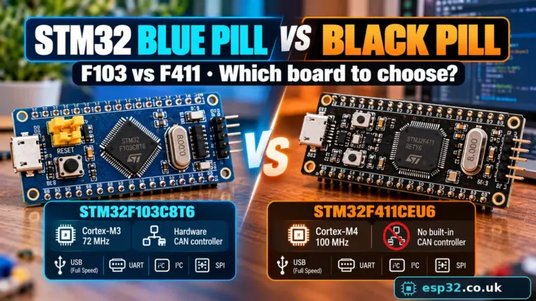
The STM32 Blue PillAliExpress price runs on 3.3 V, but that does not mean every GPIO input will be destroyed by a 5 V signal. Some STM32F103C8AliExpress price pins are explicitly marked FT (five-volt tolerant) in ST’s datasheet. Others—including the ADC pins, PB5, and PC13—are not. The difference matters when you connect an Arduino Uno, a 5 V sensor, a relay moduleAliExpress price, or a serial adapter.
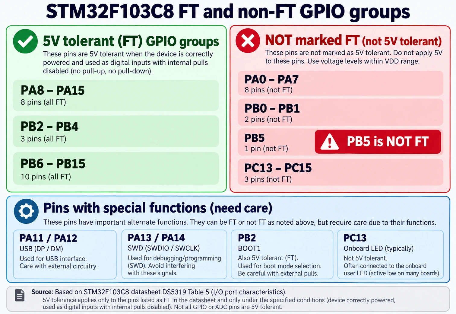
Quick answer: On an STM32F103C8 Blue Pill, PB6–PB15, PA8–PA15, PB2–PB4 are FT-labelled digital I/O pins in the chip datasheet, subject to the mode, supply and peripheral restrictions explained below. PA0–PA7, PB0, PB1, PB5, and PC13–PC15 are not listed as FT. A 5 V signal is not automatically safe just because another STM32 pin accepts it. For an ordinary 5 V analog sensor, use a correctly designed divider or buffer before connecting an ADC input.
This is a pin-level electrical guide, not a universal guarantee about every board called a “Blue Pill.” It assumes the genuine STM32F103C8T6 in the LQFP48 package, powered correctly and operated within its datasheet limits. Check chip markings and board circuitry if your board is a clone. The primary references are ST’s STM32F103x8/xB datasheet, DS5319 (pin definitions and electrical characteristics) and ST application note AN4899 (GPIO hardware configuration and tolerance).
First, separate the five voltages people confuse
A pin can be five-volt tolerant while the entire microcontroller still needs a 3.3 V supply. Before connecting anything, distinguish the following:
| Term | What it actually means | STM32F103C8 implication |
|---|---|---|
| VDD | Supply voltage for the digital MCU circuitry | Typically 3.3 V; use the datasheet operating range, never a 5 V feed to VDD |
| VDDA / VREF+ | Analog supply / ADC reference | Analog input range is tied to these rails, not to FT digital-input tolerance |
| VIH / VIL | Voltages reliably interpreted as logic HIGH and LOW | Read the thresholds for the exact input type and VDD; a 3.3 V HIGH is not guaranteed valid for every 5 V receiver |
| FT | Datasheet code for an I/O pad with conditional over-voltage tolerance | Some digital input functions can accept a 5 V HIGH when properly powered and configured |
| VOH / VOL | Guaranteed output HIGH / LOW levels at specified load current | The STM32 does not create a 5 V HIGH on its own; HIGH follows its approximately 3.3 V supply |
| Absolute maximum | Stress rating beyond which damage may occur | Not a target operating condition or a license to run at the limit |
Many Blue Pill boards expose a header marked 5V or accept 5 V USB input. That is the board’s power-input/distribution circuit, normally routed through a regulator. It does not mean that the STM32 MCU itself is powered at 5 V. Verify the particular board’s schematic before using its 5V header as a power input or output. Some boards have protection or regulator differences, and feeding two power sources together can create a reverse-current path.
“5V tolerant” is an input characteristic, not an output voltage
If PB6 is configured as a push-pull output and driven HIGH, it provides an output voltage related to VDD, not 5 V. An FT label does not turn the GPIO into a 5 V driver, a 5 V power regulator, or an unlimited surge protector. ST’s AN4899 specifically discusses tolerance in input operation and cautions against treating FT outputs (including open-drain cases) as automatically safe with 5 V applied. Always examine the mode in which your firmware—and the reset state—will leave the pin.
Which STM32F103C8 Blue Pill GPIO pins are 5V tolerant?
The authoritative answer comes from the I/O Level column of Table 5 in DS5319. A pin marked FT is a candidate for a 5 V digital input, not an ADC input or supply. Pins without FT marking should be treated as 3.3 V-domain pins, and their allowed voltage range must be checked in the electrical section of the same datasheet.
| Blue Pill pin group | FT in F103C8 datasheet? | Typical use / restrictions |
|---|---|---|
| PA0–PA7 | No | ADC-capable pins; do not feed 5 V directly |
| PA8–PA10 | Yes | Digital timer / UART signals; USART1 RX is PA10 |
| PA11–PA12 | Yes | Also USB D− / D+; never force 5 V onto them when USB peripheral/cable is in use |
| PA13–PA14 | Yes | SWDIO and SWCLK: protect debugging access; FT is not a reason to drive 5 V on debug wires |
| PA15 | Yes | Shared with JTAG/other functions; may need remapping before use as GPIO |
| PB0–PB1 | No | ADC-capable; keep within analog/digital non-FT limits |
| PB2 | Yes | BOOT1 selection at reset; do not let a 5 V external circuit disturb boot state |
| PB3–PB4 | Yes | JTAG/SWO-related after reset; remapping may be necessary |
| PB5 | No | Exception that is easy to overlook among neighbouring Port B pins |
| PB6–PB9 | Yes | Often used for I²C/timer digital functions; mind I²C bus pull-up voltage |
| PB10–PB15 | Yes | General-purpose digital/peripheral signals; verify operating mode |
| PC13–PC15 | No | PC13 commonly connects to the onboard LED; PC14/PC15 often serve low-speed crystal/RTC |
| BOOT0, NRST, 3V3, 5V, VBAT, GND | Not normal GPIO entries | Special pins and power rails have their own voltage specifications; never infer FT from a nearby GPIO |
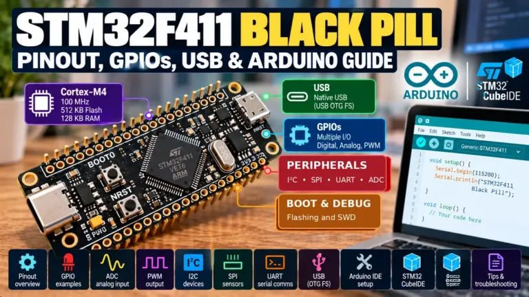
This grouping is for the familiar LQFP48 STM32F103C8 and its typical Blue Pill headers, not a pinout for other STM32F1 packages or F4 Black Pill boards. The STM32F401 and STM32F411 have different pin classifications, power domains and peripheral restrictions. Re-check their own datasheets instead of applying this table to them.
Two overlooked details: PB5 is not FT, despite PB4 and PB6 being FT; and PC13 is not FT, despite many tutorials using it as the first GPIO. ST also places a special output-drive restriction on PC13–PC15: these pins sink limited current and are not suitable for sourcing LED loads directly. The standard Blue Pill’s PC13 LED is commonly active-low, which is a separate matter from input voltage tolerance.
How to check a pin yourself, rather than trusting a colourful pinout
- Read the exact chip marking (for example STM32F103C8T6) and obtain its datasheet from ST.
- Go to Pinouts and pin description → Table 5, and find the signal by MCU pin name (
PA10,PB5, etc.), not by physical header position or board silk-screen shorthand. - Read the I/O Level column. Look for FT. A dash or blank means it is not specified as FT.
- Check the electrical characteristics, especially input-voltage limits, internal-pull restrictions and the selected peripheral function.
- Confirm the MCU is powered, the relevant pad is acting as a permitted digital input and no connected circuit (USB, debug, boot straps) conflicts with your plan.
If any of these checks fails, add level shifting or redesign the interface. This approach generalises far better than memorising somebody else’s board picture.
Conditions that make an FT pin unsafe at 5 V
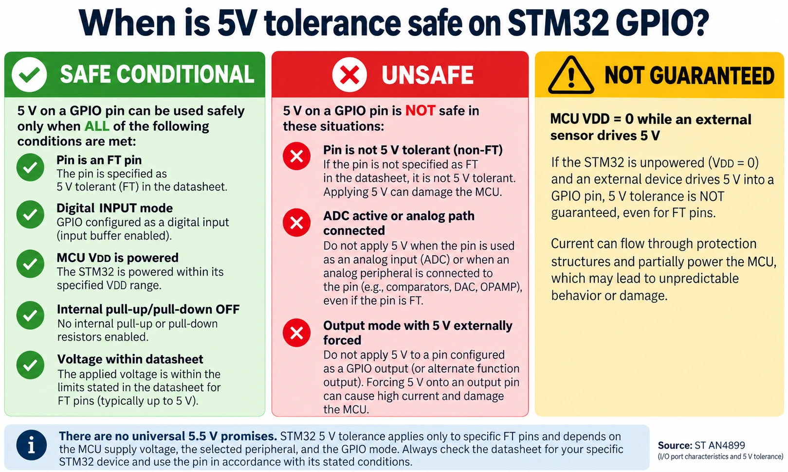
Even when DS5319 marks the pad FT, the context matters. The most common failures arise from assuming FT = permanently 5V-proof.
1. The microcontroller must be powered
ST notes in AN4899 that five-volt tolerance is not generally guaranteed when VDD is 0 V. Unpowered input-voltage limits are different, and 5 V from an always-on peripheral can back-power internal structures or exceed ratings. A sensor supplied from a separate USB charger may still be driving a pin after you unplug the Blue Pill. That is not a harmless test.
Safer design: power-cycle both sides together, gate the external signal, or use a level translator with appropriate powered-off isolation (Ioff). Do not assume that adding a resistor proves the pin is safe while unpowered; protection depends on the current path and the MCU’s specified limits.
2. Internal pull-up and pull-down settings matter
The F103 datasheet includes an explicit qualification: to sustain a voltage above VDD + 0.3 V on an FT input, its internal pull-up/pull-down resistors must be disabled. Those internal bias components connect to the lower-voltage domain. For a 5 V digital input, use a true floating input configuration as appropriate, and provide a suitable defined external bias where needed. INPUT_PULLUP is not a safe default simply because the underlying pad is FT.
Also consider reset and boot sequences. Firmware may later configure the pad differently than you intended, so document the state in which an external 5 V driver first becomes active.
3. ADC and analog peripheral functions change the rules
A non-FT ADC pin like PA0 must never be connected directly to a 0–5 V potentiometer output. On STM32 families with pads that support both FT digital operation and an analog peripheral, enabling that analog connection can remove five-volt tolerance, because the analog path connects toward VDDA/VREF+. ST explains the mechanism in AN4899; the exact switch design differs by MCU family. Do not label a channel “safe for 5 V ADC” just because its digital pad is FT.
A conventional 12-bit STM32 ADC produces readings referenced to its actual analog reference. With VDDA/VREF+ near 3.3 V, the useful measurement span is approximately 0 to 3.3 V. A 5 V signal is outside that range and may both saturate the conversion and overstress the input. Use a divider, op-amp, qualified ADC front-end, or an external ADC rated for the required signal.
4. Output modes and external pull-ups are a separate design case
A 5 V pull-up connected to a GPIO set as push-pull output HIGH can contend with the STM32’s own 3.3 V output driver. An open-drain pin is not automatically covered by the same 5 V input guarantee; output-mode tolerance must be checked against the exact MCU datasheet and ST guidance. A common I²C tutorial mistake is to configure PB6/PB7 as open-drain and simply move the bus pull-ups from 3.3 V to 5 V because those pins are FT. The safer general practice for a 3.3 V STM32 is to keep the bus pull-ups at 3.3 V when every device recognises that HIGH, or use an I²C-compatible bidirectional level shifter between 3.3 V and 5 V domains.
Safe circuit 1: reading a 5 V digital sensor or Arduino output
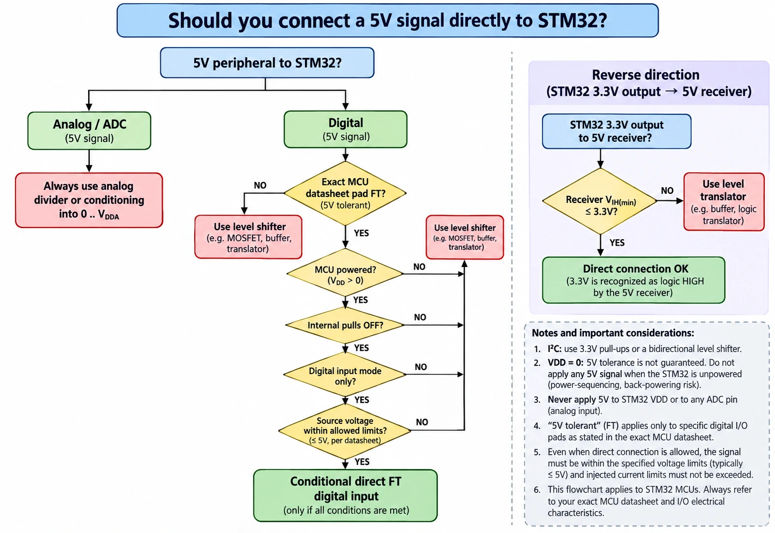
Suppose a 5 V Arduino Uno drives an ON/OFF signal to the Blue Pill. A correctly identified FT digital input may be usable directly when every specified condition holds. However, you must know the signal cannot exceed the permitted input limits, the MCU is powered, its pull resistors are off, and no boot/debug/USB function is involved. In practice, adding a level shifter or a divider often gives more margin and makes a design portable to a future MCU.
A simple passive divider for a slow, push-pull digital signal is:
- Arduino or sensor output → 4.7 kΩ upper resistor → STM32 digital input.
- STM32 input → 6.8 kΩ lower resistor → common GND.
- Arduino/sensor GND → STM32 GND. Both devices need their own appropriately regulated supplies.
At an ideal 5.0 V input, the divider produces:
Vout = Vin × Rbottom / (Rtop + Rbottom) = 5.0 × 6.8 / (4.7 + 6.8) ≈ 2.96 V.
At an ideal 5.25 V input, it produces about 3.10 V, before component tolerances. The receiving GPIO HIGH threshold must be checked, but for the F103 digital input this is normally sufficient. Use 1% resistors if precision or worst-case margins matter, and re-evaluate for the actual input range. The divider has resistance and capacitance, so do not choose it blindly for high-speed SPI, clock or fast-edge buses. Use a proper active translator where timing demands it.
With the same divider a non-FT input such as PB5 can read a 5 V digital control signal without seeing the full 5 V, assuming the divider is designed for the worst-case voltage and the unpowered condition is handled. A series resistor alone is not a voltage divider; it only limits current, and relying on internal protection structures to absorb a continuous overvoltage is poor design.
Example: digital input using Arduino STM32duino
For a simple demonstration, the example below uses PB6, which DS5319 marks FT. It leaves internal pulls off. It is not a general permission to apply 5 V in every state of the circuit, and the external source still needs a common ground.
const uint8_t signalPin = PB6;
const uint8_t ledPin = PC13;  // Common Blue Pill onboard LED, usually active-low

void setup() {
  pinMode(signalPin, INPUT);    // No MCU internal pull-up/down
  pinMode(ledPin, OUTPUT);
  digitalWrite(ledPin, HIGH);  // LED off on many Blue Pill revisions
}

void loop() {
  bool inputHigh = (digitalRead(signalPin) == HIGH);
  digitalWrite(ledPin, inputHigh ? LOW : HIGH);
  delay(20);
}
This example assumes the official STM32duino core and a Blue Pill-compatible variant. The input must be held at a defined level by the external circuit. If it floats, add an appropriate bias on the external side; the precise resistor and supply rail depend on whether you use direct FT input or level shifting. Do not use PC13 as a 5 V input simply because it appears in the same sketch: PC13 is being used only as a 3.3 V-domain LED output.
Safe circuit 2: feeding a 0–5 V sensor into an STM32 ADC
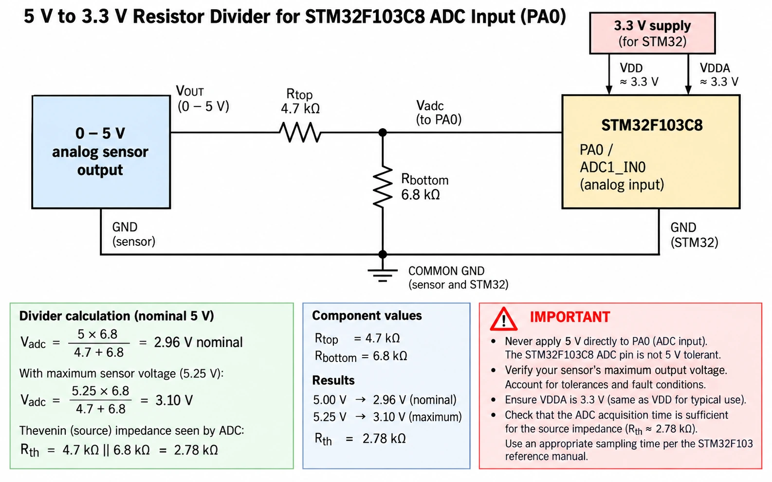
An analog sensor is a different problem: the F103’s analog inputs (for example PA0 / ADC1_IN0) are not FT. Scale the maximum sensor output to a voltage inside the ADC reference range, with tolerance for sensor overrange, resistor error and ADC supply variation.
A 4.7 kΩ high-side / 6.8 kΩ low-side divider, for instance, scales nominal 0–5 V to 0–2.96 V. At a 5.25 V input, the output is about 3.10 V. If your ADC reference falls below that, or the sensor can produce larger spikes, revise the resistor ratio and add appropriate protection. The resistors’ Thevenin source resistance is approximately 2.78 kΩ; consider that along with ADC acquisition time, pin capacitance and any filtering. A fast conversion with insufficient sample time can under-read even when the voltage itself is safe.
An example calculation from a 12-bit ADC, if the actual ADC reference is 3.300 V and there are no significant calibration or loading errors:
Rtop = 4.7 kΩ, Rbottom = 6.8 kΩ
Divider ratio k = 6.8 / (4.7 + 6.8) = 0.59130
ADC full scale = 4095 counts
V_ADC  = ADC_counts / 4095 × VREF_actual
V_IN   = V_ADC / k
Example: ADC_counts = 3000 → V_ADC ≈ 2.418 V → V_IN ≈ 4.09 V
This is not a substitute for calibration. Check whether the sensor output is ratiometric with its supply, estimate resistor tolerance, measure VREF/VDDA rather than assuming 3.300 V, and choose a sufficiently long ADC sampling time for your source impedance. Protect against transients or accidental overvoltage if this is installed outside a lab. For continuously monitoring an automotive or industrial 5 V signal, consider a dedicated protected input circuit or ADC front-end.
Connecting common 5 V peripherals: which approach works?
| External device or signal | Suggested approach | What to avoid |
|---|---|---|
| Arduino Uno 5 V digital output | Level shift to 3.3 V; or qualified FT digital input with the conditions checked | Direct connection to non-FT GPIO or to ADC |
| 5 V analog potentiometer/sensor | Calibrated divider or analog conditioning into an ADC pin | Feeding a 0–5 V signal straight into PA0–PA7/PB0/PB1 |
| 5 V HC-SR04 ECHO | Suitable divider/translator on ECHO into GPIO | Assuming all Blue Pill pins are FT |
| 5 V UART adapter TX | Prefer a 3.3 V-level adapter; where unavoidable verify MCU RX FT, power sequence and mode | RS-232 ±voltage levels, or 5 V TX into an arbitrary MCU RX pin |
| STM32 3.3 V TX → 5 V receiver | Check receiver VIH; use up-shifter/buffer if needed | Assuming every 5 V CMOS input reads 3.3 V HIGH |
| I²C module with 5 V pull-ups | Move compatible bus pull-ups to 3.3 V or use bidirectional I²C level shifter | “PB6 is FT, therefore a 5 V pull-up is always safe” |
| 5 V SPI module | Translate the 5 V-to-3.3 V signals; check high-speed timings and return-path ground | Slow resistor dividers on fast edges without testing |
| 5 V relay-board control input | Check module’s trigger circuit and input current; often use a transistor/MOSFET driver | Driving a coil directly or assuming 3.3 V will trigger any 5 V module |
| 5 V PWM or encoder output | Dedicated input protection/translator for noisy cables; FT input only when fully qualified | Feeding inductive transients straight to GPIO |
Special case: I²C pull-ups and open-drain outputs
Because I²C devices normally pull the bus LOW and otherwise release it, the bus HIGH voltage comes from the pull-up resistors. If a BME280 breakout and an STM32 board are both designed for 3.3 V logic, pull SDA and SCL up to 3.3 V. Some “5 V-compatible” breakout boards already include translators; others do not. A pull-up to the breakout’s 5 V rail is not equivalent to a 3.3 V pull-up. Identify the module’s schematic rather than deciding from the sensor IC name alone. Choose I²C translator parts suitable for bidirectional open-drain signaling; a generic one-direction buffer may not work.
Special case: UART and USB lines
The STM32F103C8’s PA10 (USART1_RX) is FT in DS5319, but using a 3.3 V logic-level USB-to-UART interface is still the more portable approach. It avoids power-up sequencing and clone-configuration surprises. Always share ground, cross adapter TX to MCU RX, and do not connect an RS-232 interface directly; RS-232 is a different electrical standard. The PA11/PA12 USB D−/D+ pins are FT-labelled in the digital I/O table, but USB is a dedicated signalling interface, not a general 5 V control input. VBUS must be handled according to the USB and board power circuitry; it must not be shorted to D+ or D−.
Three common projects and their actual voltage pitfalls
HC-SR04 ultrasonic ranging module
Many conventional HC-SR04 ultrasonic modules accept a 5 V supply and return an ECHO pulse approaching 5 V. The TRIG input is separate: a 3.3 V output may be accepted by a particular module, but verify its input-high specification or use a buffer. For ECHO, choose a verified FT digital input or a logic divider or translator; I would still favour a divider for a tutorial intended to work across different microcontrollers. With the 4.7 kΩ / 6.8 kΩ example, ECHO drops to roughly 2.96 V at a nominal 5 V level. A common ground and a suitable microsecond-resolution timer input are also required. Do not feed ECHO into PA0 just because that pin is convenient for breadboarding.
The module may generate fast pulses. Your chosen divider, cable capacitance and MCU input-filter settings influence timing and edges. A few centimetres on the bench and a five-metre cable routed next to a motor are not the same electrical problem. If this is a noisy installation, consider transient clamps or a buffer designed for the application.
5 V switch or proximity sensor
Check whether the output is push-pull, open collector/open drain, PNP or NPN. A simple NPN open-collector sensor may let you choose a 3.3 V pull-up on the STM32 side, avoiding a 5 V HIGH entirely, provided the sensor output stage is rated for this arrangement and shares a suitable ground. A push-pull PNP industrial sensor, in contrast, might switch to a supply much higher than 5 V. It needs an industrial-rated input circuit, often an optocoupler, comparator or protected voltage divider. Never infer safety merely from the label “digital sensor.”
Level-shifter modules sold for I²C and SPI
Common four-channel MOSFET-based bidirectional boards are primarily intended for open-drain buses such as I²C. They may appear to work with slow UART or SPI in a short test, but their edge speed depends on pull-ups, FET capacitance and wiring. For fast SPI choose a translator with proper directionality, bandwidth and logic thresholds. Watch for modules whose jumper connects a 5 V rail to the low-voltage side accidentally. Measure the actual HV and LV rail pins before attaching the STM32, and avoid hot-plugging signals before ground is established.
A meter reading is necessary but not sufficient
A multimeter may show a perfectly safe 2.96 V on a divider while an oscilloscope reveals negative undershoot, overshoot beyond 3.3 V, or power-off leakage during switching. Pay particular attention to inductive loads, long cables, reset timing and separate power supplies. If the signal is slow, a divider and a shared ground can be a neat engineering solution. If the signal is fast, safety-critical, isolated or connected outside the enclosure, use an interface designed and tested for those conditions.
The other direction: will a 3.3 V STM32 output control 5 V logic?
This question is independent of 5 V input tolerance. A 3.3 V push-pull output may work with a receiver whose input-high threshold is low enough. Many TTL-compatible 5 V logic inputs recognise about 2 V as HIGH, but other CMOS inputs may demand a much higher fraction of their own 5 V supply. Look up VIH(min) in the receiver’s datasheet; do not assume a 5 V-powered sensor, shift register or LED controller shares a particular threshold.
For a robust logic HIGH at a true 5 V level, use an appropriate 3.3-to-5 V translator/buffer powered from both domains, with output-enable/power-off behaviour compatible with your startup sequence. For a unidirectional MOSFET, gate driver or optocoupler interface, calculate input current, resistor values, polarity, duty cycle and rise/fall times. Never connect a motor, relay coil or large LED load directly to an STM32 GPIO, regardless of whether that pin is FT.
What about STM32F401 and STM32F411 Black Pill boards?
FT pin classification is not portable by board colour or family nickname. A Black Pill may contain an STM32F401CC, F401CE, F411CE or a different MCU. These devices have different package/pin maps from the F103 and may distinguish FT, TT, TC, FT_a or other pad structures in their own datasheets. Check the precise ordering code, then the pin table, the maximum input voltage conditions and the active alternate function.
The safest transferable rules are: never feed 5 V into a 3.3 V power pin, never assume an ADC input can directly measure 5 V, do not use an FT input as a guarantee in output/analog/unpowered states, and do not disturb SWD, reset, boot or USB lines. Where the interface cannot tolerate uncertainty, place a dedicated translator or protection front-end at the board boundary.
A troubleshooting checklist before connecting 5 V
A little time with a multimeter often prevents hours of debugging—or a dead microcontroller.
- Identify the exact MCU. Read the chip marking and datasheet for the specific package, not just the seller’s board name.
- Measure VDD/VDDA. Confirm a stable correct MCU supply; a powered USB connector does not guarantee the regulator is healthy.
- Read the pad class. For F103C8, find FT in DS5319 Table 5. Remember PB5 is not FT.
- Write down the pin mode. Digital input? Internal pulls OFF? Analog peripheral disconnected? Will the firmware ever drive this pin?
- Check the external source at maximum and minimum. A “5 V” line may overshoot, ring or remain powered when the STM32 is off.
- Check startup order. If the peripheral may be powered first, use translation or power-off isolation rather than assuming FT works with VDD=0.
- Assess ground and cable conditions. Long cables and separate power adapters can introduce ground offsets, ESD or inductive transients.
- Design the interface. Use a verified digital translator, correctly calculated divider, protected input or suitable driver; do not rely on protection diodes.
- Test with current-limited supplies. Verify the actual voltage at the MCU pin during startup, operation and power-down, using an oscilloscope for fast signals.
- Check the receiving logic threshold. A signal that is safe electrically still may not register as HIGH, especially in the 3.3 V → 5 V direction.
Frequently asked questions
Can I connect a 5 V Arduino output to STM32 PB6 directly?
PB6 is FT-labelled on a genuine STM32F103C8, so a qualified 5 V digital input application may permit it while the MCU is properly powered, the pin is in an appropriate input configuration and its internal pull resistors are disabled. The external signal must stay within the device’s datasheet limits, including transient and power-off cases. For a plug-and-play project where these conditions are unknown, use a 3.3 V level translator or divider.
Is PA0 on the Blue Pill five-volt tolerant?
No. PA0 is an ADC-capable pin and is not marked FT in the F103C8 pin-definition table. Scale an analog signal to the actual ADC reference range. For a 5 V digital source into PA0 as GPIO, level-shift it too.
Is PC13 5V tolerant? Can it drive a relay?
No, PC13 is not FT. It is also a relatively restricted output on the F103. Its common onboard LED is low-current and typically active-low. Use a driver transistor or interface IC for a relay; do not connect a relay coil to PC13 directly.
Is every Blue Pill Port B pin 5V tolerant?
No. In the F103C8 pin table, PB0, PB1 and PB5 are not FT. Other exposed Port B pins are listed FT, but boot, debug and alternate-function restrictions still apply. Do not apply one rule to the entire port.
If a pin says FT, can I put 5 V on it before powering the STM32?
Do not assume so. ST explicitly warns that 5 V tolerance is not generally guaranteed when VDD is absent. Either sequence supplies together, hold the signal off, or use a translator with documented powered-off protection.
Can an STM32 output 5 V from a 5V-tolerant GPIO?
No. FT describes an input-voltage property. With VDD around 3.3 V, a push-pull HIGH output is associated with that supply and load—not a 5 V level. Use a step-up level shifter for a receiver that requires 5 V logic HIGH.
Can I use 5 V I²C pull-ups on PB6/PB7?
The safe default is 3.3 V bus pull-ups or a proper bidirectional I²C translator. ST’s tolerance conditions for input pads do not by themselves establish that an output configured as open-drain is safe at 5 V. Check both the MCU electrical documentation and the module’s pull-up circuitry.
Final recommendation
The useful rule is not “STM32 is 3.3 V, so 5 V always destroys it,” nor “STM32 has 5V-tolerant pins, so 5 V is fine.” It is read the pad class, verify its current electrical mode and supply state, and design for worst-case voltages. The STM32F103C8 does have genuinely FT-labelled pins, but its common ADC pins and PC13 are not among them, and PB5 is the easy-to-miss exception. For mixed-voltage hardware you intend to reuse or publish as a wiring tutorial, a small amount of deliberate level shifting is usually worth more than the cost savings of one omitted component.
Further reading: STM32 for Beginners · How to Program Blue Pill with ST-LINK · Blue Pill Arduino IDE Guide · Blue Pill USB Troubleshooting · ST’s AN4899 · STM32F103C8 datasheet.