An STM32PriceAliExpress price timer can generate a stable PWM output while your program reads sensors, updates a display or waits for a serial command. A second timer can record incoming edges and measure their spacing. Once you understand the clock feeding each timer, the same registers explain LEDPrice dimming, servoPriceAliExpress price control, frequency measurement and regularly scheduled sampling.
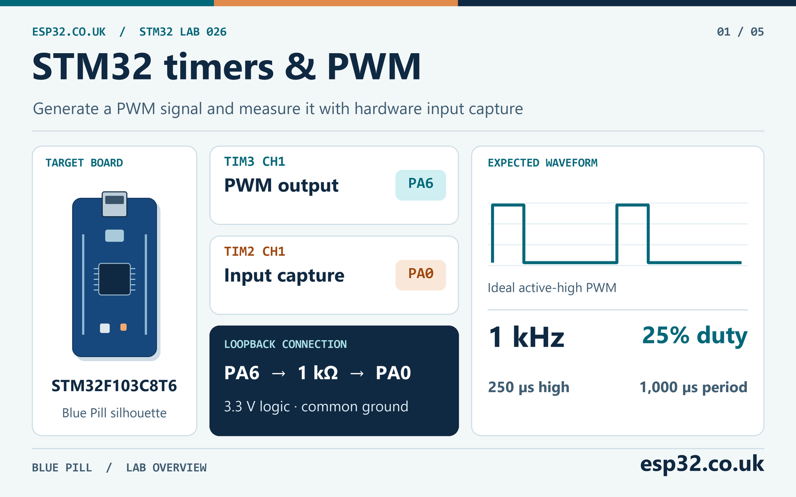
In this guide, you will build a reproducible STM32F103C8T6AliExpress price Blue Pill experiment. TIM3 generates a 1 kHz, 25% duty-cycle signal on PA6. A short connection to PA0 lets TIM2 measure the signal using hardware input capture. You will calculate every timer setting, change the PWM duty cycle, examine counter rollover and recognise measurements that have become stale.
Quick answer. With a 72 MHz TIM3 clock, set PSC = 71, ARR = 999 and CCR1 = 250. Select PWM mode 1, active-high polarity and the default PA6 route for TIM3 channel 1. Start the channel with HAL_TIM_PWM_Start(). For frequency measurement, configure TIM2 channel 1 on PA0 with a 1 MHz counter and subtract consecutive rising-edge captures.
This article targets the genuine STM32F103C8T6 and STM32CubeF1 HAL. Board clones, STM32F4 parts and other STM32 families need their own clock and pin checks. The packaged example is an integration module for a fresh CubeMX-generated C project. Its source and arithmetic have been reviewed, while compilation and physical board measurements remain part of the bring-up procedure below.
Choose the timer and reserve its pins
The STM32F103C8 has TIM1 plus three general-purpose timers, TIM2, TIM3 and TIM4. These four peripheral counters are 16-bit on this device. TIM1 adds advanced output features used in motor-control designs. SysTick and the watchdogs account for the remaining timers in the datasheet’s headline total. Read the exact device specification before adapting code from a chip with a 32-bit TIM2. ST STM32F103x8/xB datasheet
| Peripheral | Default channel pins on the LQFP48 device | Use in this experiment |
|---|---|---|
| TIM1 | CH1 PA8, CH2 PA9, CH3 PA10, CH4 PA11 | Available for a later project |
| TIM2 | CH1 PA0, CH2 PA1, CH3 PA2, CH4 PA3 | Rising-edge capture on PA0 |
| TIM3 | CH1 PA6, CH2 PA7, CH3 PB0, CH4 PB1 | PWM output on PA6 |
| TIM4 | CH1 PB6, CH2 PB7, CH3 PB8, CH4 PB9 | Available for a later project |
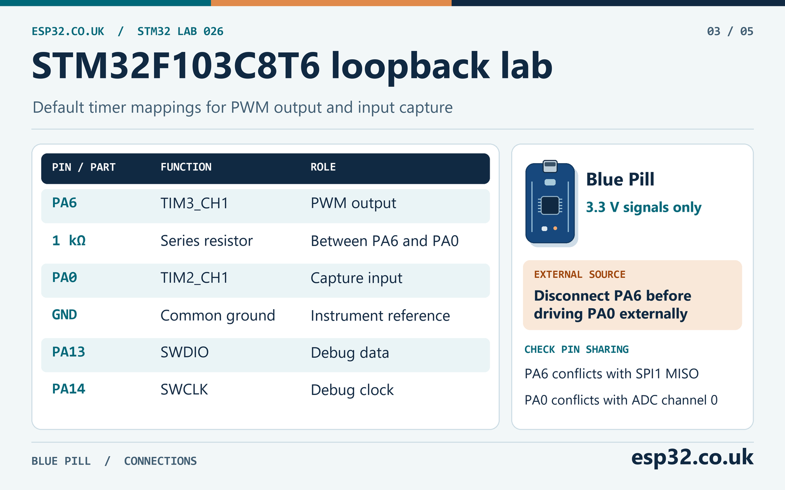
These are default mappings. Remapping can move channels, sometimes onto pins unavailable on the package. PA0 is also ADC channel 0, and PA6 is also SPI1 MISO. Disconnect the previous ADC or SPI experiment before using those pads here. A peripheral assignment belongs to the entire project, so combining two working examples requires reviewing their shared resources.
Use a genuine ST-LINK or another compatible SWD programmer, a Blue Pill with a verified 8 MHz HSE crystal, a short jumper and a stable supply. An oscilloscope or logic analyser makes the output independently observable. Keep PA13 and PA14 available for SWD. Check header labels against the board before applying power. Our existing pinout guide provides the broader board reference. Blue Pill pinout guide
Understand the clock before choosing a prescaler
There are three relevant rates. SYSCLK feeds the clock tree, the APB bus clocks feed peripheral interfaces, and a timer kernel clock feeds the timer’s own prescaler. They can have different numerical values. Calculating from the CPU frequency alone produces correct results only when the rest of the clock configuration happens to match that assumption.
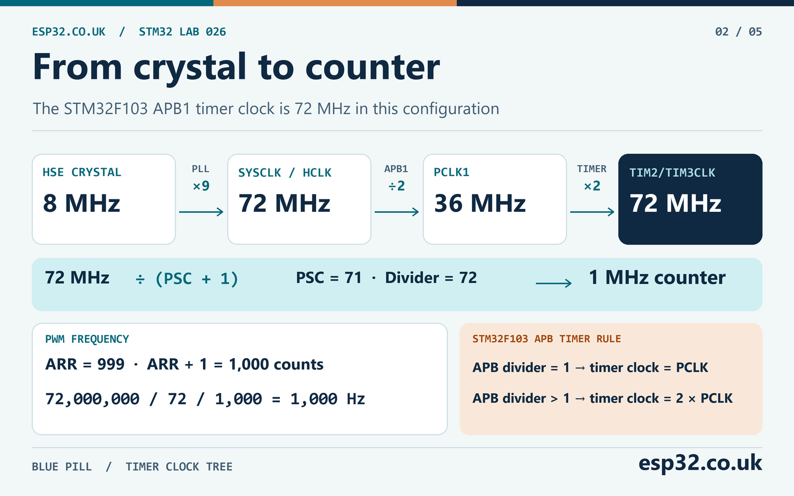
For this lab, configure an 8 MHz HSE source multiplied by nine. Use a 72 MHz system and AHB clock, APB1 divided by two, and APB2 undivided. TIM2 and TIM3 are attached to APB1. On this STM32F1 clock tree, the timer clock equals PCLK when the APB prescaler is one, and equals twice PCLK when that prescaler is greater than one. Consequently, PCLK1 is 36 MHz while TIM2CLK and TIM3CLK are 72 MHz. ST RM0008 reference manual, RCC clock tree
| Clock setting | Selected value | Result |
|---|---|---|
| HSE crystal | 8 MHz | PLL source |
| PLL multiplier | ×9 | SYSCLK 72 MHz |
| AHB prescaler | /1 | HCLK 72 MHz |
| APB1 prescaler | /2 | PCLK1 36 MHz |
| APB1 timer multiplier | ×2 | TIM2/TIM3 72 MHz |
| Timer prescaler register | 71 | Counter advances at 1 MHz |
At 1 MHz, one counter increment represents one microsecond. That makes the first experiment easy to inspect. A 1,000-count PWM cycle lasts 1,000 microseconds. A capture difference of 1,000 therefore represents the same one-millisecond period.
The timer’s ClockDivision setting is a separate control associated with its sampling/dead-time clock. It is not a replacement for the prescaler that sets the counter rate. Leave it at TIM_CLOCKDIVISION_DIV1 here. Also check the configured HSE_VALUE against the physical crystal. Software frequency reporting depends on those constants and cannot discover a wrongly labelled oscillator.
Calculate frequency, duty cycle and resolution
For an internally clocked timer counting upward in edge-aligned PWM mode, use these relationships.
counter_hz = timer_hz / (PSC + 1)
pwm_hz = counter_hz / (ARR + 1)
period_seconds = (PSC + 1) * (ARR + 1) / timer_hz
duty_fraction = CCR / (ARR + 1)
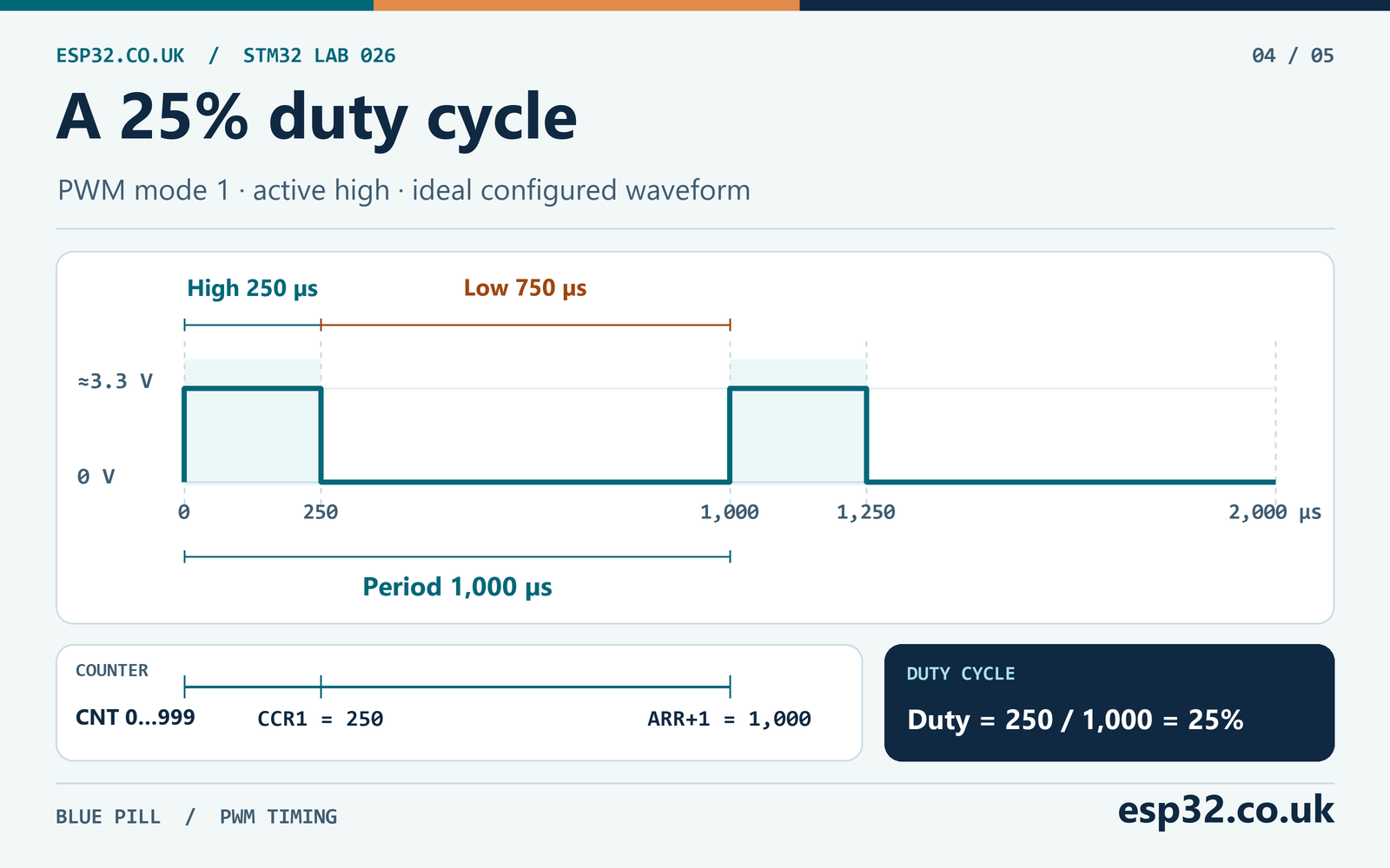
The counter visits every value from zero through ARR, inclusive. With ARR equal to 999, there are 1,000 time slots. In active-high PWM mode 1, a compare value of 250 makes the output high for the first 250 slots. The output then stays low for the remaining 750 slots. This establishes both a 1 kHz frequency and a 25% duty cycle.
| Target | PSC | ARR | CCR | Counter rate | High time |
|---|---|---|---|---|---|
| 1 kHz at 25% | 71 | 999 | 250 | 1 MHz | 250 µs |
| 1 kHz at 50% | 71 | 999 | 500 | 1 MHz | 500 µs |
| 20 kHz at 50% | 0 | 3599 | 1800 | 72 MHz | 25 µs |
| 50 Hz servo frame, 1.5 ms pulse | 71 | 19999 | 1500 | 1 MHz | 1,500 µs |
These are independently calculated configurations. The supplied duty setter assumes the first row’s 1,000-count period. If you change ARR for another experiment, update the setter’s scaling as well. A function that multiplies percentage by ten cannot control a 20,000-count servo frame correctly.
PWM resolution is set by the number of available time slots. The 1 kHz example provides steps of 0.1 percentage point at the register level. The public percentage setter deliberately exposes whole percentages for clarity. At 20 kHz with PSC zero, 3,600 slots provide finer duty steps than a 1 MHz counter would provide at the same output frequency.
For a frequency that does not divide evenly, choose integer register values and calculate the achieved frequency. Report the error as (achieved - target) / target × 100%. For example, PSC zero and ARR 1632 give approximately 44,090.63 Hz from 72 MHz, about −0.0212% relative to 44,100 Hz. Crystal tolerance adds another contribution. More decimal places in the calculation do not increase physical accuracy.
Connect the loopback experiment
Power the board normally and connect PA6 to PA0 through approximately 1 kΩ. The resistor offers modest protection against an accidental output conflict during experimentation. Both pins belong to the same board and already share ground. Connect the measurement instrument’s ground to board ground. Keep the jumper short and avoid attaching any external source while PA6 drives the connection.
| Connection | Purpose | Check before starting |
|---|---|---|
| PA6 through 1 kΩ to PA0 | TIM3 output reaches TIM2 input | PA6 output, PA0 input |
| Instrument channel to PA6 | Independent waveform observation | Instrument accepts 3.3 V logic |
| Instrument ground to GND | Common measurement reference | Secure ground connection |
| ST-LINK SWDIO to PA13 | Programming and debugging | Preserve Serial Wire mode |
| ST-LINK SWCLK to PA14 | Debug clock | Check programmer pin labels |
PA0 and PA6 are not marked FT in the device’s pin table. Use signals confined to the board’s 3.3 V logic domain. A function generator’s amplitude setting can depend on whether it assumes a 50 Ω load, so verify the actual signal and offset before connecting it. Negative-going signals also need appropriate conditioning.
For an external frequency source, remove the PA6 jumper, connect the source to PA0 and connect grounds. Start with a clean 3.3 V push-pull square wave. Open-drain outputs need a suitable pull-up to 3.3 V, whereas slow mechanical switches need debouncing. Our voltage-level guide explains the broader electrical checks. STM32 GPIO voltage levels
Create the CubeMX project without duplicate timer owners
Start a C project for STM32F103C8Tx. Enable Serial Wire debugging and configure the HSE crystal and clock tree described above. Leave the HAL timebase on SysTick. This module owns TIM2 and TIM3, so leave both peripherals disabled in CubeMX and let the module initialise them. That also avoids generating a second TIM2 interrupt handler.
Generate the project for your installed STM32CubeIDE workflow. Copy timer_lab.c into Core/Src and timer_lab.h into Core/Inc. Enable HAL_TIM_MODULE_ENABLED in stm32f1xx_hal_conf.h, ensure the timer HAL header is included through that configuration, and add the package’s stm32f1xx_hal_tim.c and stm32f1xx_hal_tim_ex.c driver sources to the build if CubeMX omitted them. Use both files from the same STM32CubeF1 package as the other HAL drivers.
The module’s hardware configuration corresponds to the following settings. They are a reference for inspecting the code or building a separate CubeMX-owned implementation.
| Setting | TIM3 output | TIM2 input |
|---|---|---|
| Counter mode | Up | Up |
| Internal counter clock | 72 MHz / 72 | 72 MHz / 72 |
| PSC | 71 | 71 |
| ARR | 999 | 65535 |
| Channel | CH1, PWM mode 1 | CH1, direct TI1 |
| Polarity | Active high | Rising edge |
| Compare or input divider | CCR1 250 | Capture every edge |
| Input filter | Not applicable | Zero for clean loopback |
| Auto-reload preload | Enabled | Disabled |
| Interrupt | None required | TIM2 capture interrupt |
Keep generated HAL_Init(), SystemClock_Config(), startup assembly and SysTick handling. Add the calls below inside the appropriate user-code sections. The variables are intentionally visible to the debugger. Inspect them with live expressions while execution continues, because stopping the processor changes interrupt servicing.
/* USER CODE BEGIN Includes */
#include "timer_lab.h"
/* USER CODE END Includes */

/* USER CODE BEGIN PV */
volatile uint32_t measured_hz;
volatile uint32_t measured_period_us;
volatile uint32_t measurement_status;
volatile uint32_t capture_overruns;
/* USER CODE END PV */

/* USER CODE BEGIN 2: after generated clock and GPIO setup */
TimerLab_Init();
/* USER CODE END 2 */

/* Inside the existing while (1) body */
LabReading sample = TimerLab_Read();
measurement_status = sample.status;
capture_overruns = sample.overcapture_events;
measured_period_us = sample.period_ticks;
measured_hz = 0U;
if (sample.status == LAB_VALID) {
    measured_hz = 1000000U / sample.period_ticks;
}
HAL_Delay(100U);
At the default output, the expected period is approximately 1,000 microseconds and the expected frequency is approximately 1,000 Hz. Integer division truncates the displayed frequency. For a more precise display, perform floating-point conversion in the main loop or calculate scaled integer units. Keep serial formatting and blocking transmissions out of the interrupt handler. The existing UART tutorial covers adding a serial output after this lab works. STM32 UART tutorial
Run the HAL timer module
The module checks the configured timer clock, enables its peripheral clocks, selects the default pin routes and starts capture before PWM. It uses HAL for setup and start operations. Its small TIM2 interrupt handler reads the capture register directly so it can examine overcapture status around that read. This implementation owns TIM2’s interrupt path, including its flags.
The header defines the observable measurement states. LAB_VALID means a recent, accepted pair of edges under the stated operating assumptions. Treat all other states as unavailable measurement data. The cumulative overcapture counter remains useful even after later samples recover.
#ifndef TIMER_LAB_H
#define TIMER_LAB_H

#include "stm32f1xx_hal.h"

typedef enum {
    LAB_WAITING = 0,
    LAB_ACQUIRING,
    LAB_VALID,
    LAB_OUT_OF_RANGE,
    LAB_OVERCAPTURE,
    LAB_STALE
} LabStatus;

typedef struct {
    uint32_t period_ticks;
    uint32_t last_edge_ms;
    uint32_t overcapture_events;
    uint32_t status;
} LabReading;

void TimerLab_Init(void);
void TimerLab_SetDuty(uint32_t percent);
LabReading TimerLab_Read(void);

#endif
#include "main.h"
#include "timer_lab.h"
static TIM_HandleTypeDef pwm_timer;
static TIM_HandleTypeDef capture_timer;
static volatile LabReading reading;
static uint16_t previous_capture;
static uint32_t previous_edge_ms;
static uint8_t have_previous;
static void require_ok(HAL_StatusTypeDef status)
{
if (status != HAL_OK) {
Error_Handler();
}
}
void TimerLab_Init(void)
{
RCC_ClkInitTypeDef clocks = {0};
uint32_t flash_latency;
HAL_RCC_GetClockConfig(&clocks, &flash_latency);
uint32_t timer_hz = HAL_RCC_GetPCLK1Freq();
if (clocks.APB1CLKDivider != RCC_HCLK_DIV1) {
timer_hz *= 2U;
}
if (timer_hz != 72000000U) {
Error_Handler();
return;
}
__HAL_RCC_AFIO_CLK_ENABLE();
__HAL_RCC_GPIOA_CLK_ENABLE();
__HAL_RCC_TIM2_CLK_ENABLE();
__HAL_RCC_TIM3_CLK_ENABLE();
/* Write SWJ_CFG explicitly because its readback is not reliable. */
MODIFY_REG(AFIO->MAPR,
AFIO_MAPR_TIM2_REMAP | AFIO_MAPR_TIM3_REMAP | AFIO_MAPR_SWJ_CFG,
AFIO_MAPR_SWJ_CFG_JTAGDISABLE);
GPIO_InitTypeDef gpio = {0};
gpio.Pin = GPIO_PIN_6;
gpio.Mode = GPIO_MODE_AF_PP;
gpio.Speed = GPIO_SPEED_FREQ_LOW;
HAL_GPIO_Init(GPIOA, &gpio);
gpio.Pin = GPIO_PIN_0;
gpio.Mode = GPIO_MODE_INPUT;
gpio.Pull = GPIO_PULLDOWN;
HAL_GPIO_Init(GPIOA, &gpio);
pwm_timer.Instance = TIM3;
pwm_timer.Init.Prescaler = 71U;
pwm_timer.Init.CounterMode = TIM_COUNTERMODE_UP;
pwm_timer.Init.Period = 999U;
pwm_timer.Init.ClockDivision = TIM_CLOCKDIVISION_DIV1;
pwm_timer.Init.AutoReloadPreload = TIM_AUTORELOAD_PRELOAD_ENABLE;
require_ok(HAL_TIM_PWM_Init(&pwm_timer));
TIM_OC_InitTypeDef output = {0};
output.OCMode = TIM_OCMODE_PWM1;
output.Pulse = 250U;
output.OCPolarity = TIM_OCPOLARITY_HIGH;
output.OCFastMode = TIM_OCFAST_DISABLE;
require_ok(HAL_TIM_PWM_ConfigChannel(&pwm_timer, &output, TIM_CHANNEL_1));
TIM3->EGR = TIM_EGR_UG;
TIM3->SR = 0U;
capture_timer.Instance = TIM2;
capture_timer.Init.Prescaler = 71U;
capture_timer.Init.CounterMode = TIM_COUNTERMODE_UP;
capture_timer.Init.Period = 65535U;
capture_timer.Init.ClockDivision = TIM_CLOCKDIVISION_DIV1;
capture_timer.Init.AutoReloadPreload = TIM_AUTORELOAD_PRELOAD_DISABLE;
require_ok(HAL_TIM_IC_Init(&capture_timer));
TIM_IC_InitTypeDef input = {0};
input.ICPolarity = TIM_INPUTCHANNELPOLARITY_RISING;
input.ICSelection = TIM_ICSELECTION_DIRECTTI;
input.ICPrescaler = TIM_ICPSC_DIV1;
input.ICFilter = 0U;
require_ok(HAL_TIM_IC_ConfigChannel(&capture_timer, &input, TIM_CHANNEL_1));
TIM2->EGR = TIM_EGR_UG;
TIM2->SR = 0U;
HAL_NVIC_SetPriority(TIM2_IRQn, 1U, 0U);
HAL_NVIC_ClearPendingIRQ(TIM2_IRQn);
HAL_NVIC_EnableIRQ(TIM2_IRQn);
require_ok(HAL_TIM_IC_Start_IT(&capture_timer, TIM_CHANNEL_1));
require_ok(HAL_TIM_PWM_Start(&pwm_timer, TIM_CHANNEL_1));
}
void TimerLab_SetDuty(uint32_t percent)
{
if (percent > 100U) {
percent = 100U;
}
__HAL_TIM_SET_COMPARE(&pwm_timer, TIM_CHANNEL_1, percent * 10U);
}
/* This handler owns TIM2. Do not also call HAL_TIM_IRQHandler for TIM2. */
void TIM2_IRQHandler(void)
{
uint32_t flags = TIM2->SR;
if ((flags & TIM_SR_CC1IF) == 0U) {
return;
}
uint16_t captured = (uint16_t)TIM2->CCR1;
uint32_t now = HAL_GetTick();
reading.last_edge_ms = now;
if (((flags | TIM2->SR) & TIM_SR_CC1OF) != 0U) {
__HAL_TIM_CLEAR_FLAG(&capture_timer, TIM_FLAG_CC1OF);
reading.overcapture_events++;
reading.period_ticks = 0U;
reading.status = LAB_OVERCAPTURE;
have_previous = 0U;
return;
}
if (have_previous == 0U) {
reading.period_ticks = 0U;
reading.status = LAB_ACQUIRING;
have_previous = 1U;
} else {
uint16_t elapsed = (uint16_t)(captured - previous_capture);
uint32_t gap_ms = now - previous_edge_ms;
if (gap_ms > 55U || elapsed < 100U || elapsed > 50000U) {
reading.period_ticks = 0U;
reading.status = LAB_OUT_OF_RANGE;
} else {
reading.period_ticks = elapsed;
reading.status = LAB_VALID;
}
}
previous_capture = captured;
previous_edge_ms = now;
}
LabReading TimerLab_Read(void)
{
uint32_t primask = __get_PRIMASK();
__disable_irq();
LabReading result = reading;
uint32_t now = HAL_GetTick();
__set_PRIMASK(primask);
if (result.status != LAB_WAITING &&
(uint32_t)(now - result.last_edge_ms) > 100U) {
result.period_ticks = 0U;
result.status = LAB_STALE;
}
return result;
}Call initialisation once after reset. Keep the generated Error_Handler() available and set a breakpoint there during bring-up. A clock mismatch or a failed HAL configuration enters that handler. TIM2 and TIM3 must be exclusively available to this module, including their handles, interrupts and pin assignments.
The reviewed HAL implementation enables channel compare preload during PWM channel configuration. The explicit update event transfers initial settings before the timer starts, and startup status flags are cleared while it is stopped. This helps make the first full period consistent with later periods. ST STM32F1 timer HAL source, v1.1.10
Change duty cycle without restarting the waveform
Call TimerLab_SetDuty(50U) from ordinary application code to request 50%. With compare preload enabled, a new compare value takes effect at the timer’s update boundary. You can update a brightness command without resetting the counter for every change. Restarting the timer repeatedly would change the timing of the output frame.
For this specific ARR of 999, CCR zero produces continuous low, and CCR 1000 produces continuous high in PWM mode 1. There are no repeated rising edges at those endpoints. The frequency display will eventually report stale data even though the output level is exactly what you requested. Inspect the output voltage or scope trace to distinguish this condition from a wiring fault.
With a 16-bit ARR of 65535, the corresponding ARR+1 value is 65536 and cannot be represented in a 16-bit compare register. An application requiring that endpoint must choose an appropriate period or deliberately force the output state. Endpoint behaviour should be part of the design, especially when a load reacts differently to an inactive pin and a driven low level.
Preload also matters when changing frequency. PSC is buffered, and ARR can be buffered. Updating several registers while the timer runs may allow an update event between those writes. For a simple lab, stop the output, change PSC/ARR/CCR, generate an update event, clear startup flags and restart. A phase-continuous control system needs a coordinated update strategy. ST AN4776 timer application note
Understand capture subtraction and counter rollover
An input edge copies the counter into a capture register. Reading that stored timestamp avoids using interrupt arrival time as the fine timing measurement. The processor may enter the handler slightly later, but the hardware captured the counter at the accepted edge. The input synchroniser, filtering and clock quantisation still affect the result.
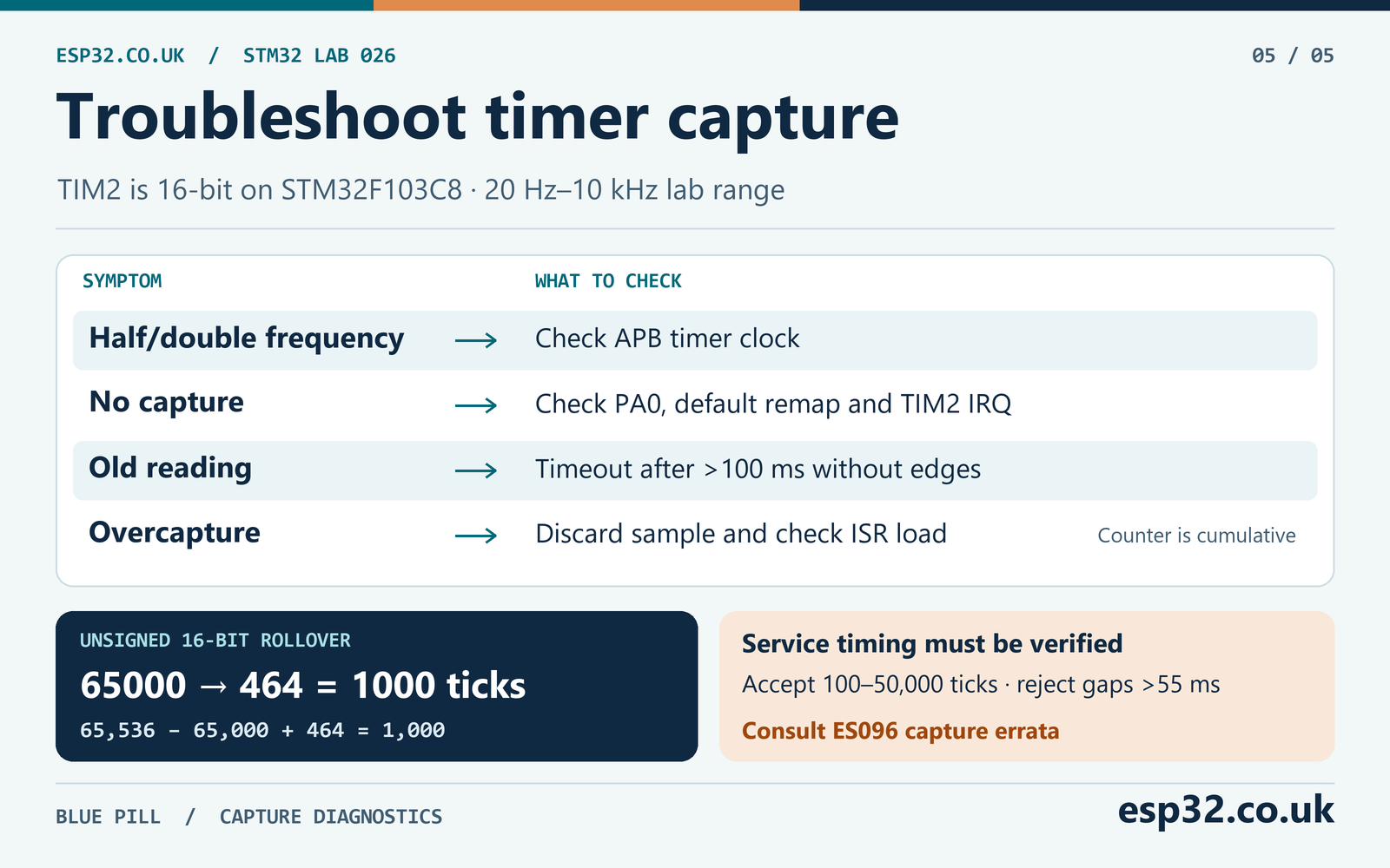
With TIM2 ARR equal to 65535, the counter wraps every 65,536 microseconds. Suppose consecutive rising edges are captured at 65,000 and 464. Unsigned 16-bit subtraction gives 1,000, which correctly represents the interval across the wrap. Changing ARR to a smaller number would invalidate that particular modulo-65536 calculation.
| First capture | Second capture | Unsigned 16-bit difference | Interpretation |
|---|---|---|---|
| 12000 | 13000 | 1000 | Ordinary 1 ms period |
| 65000 | 464 | 1000 | Same period across counter rollover |
| 1000 | 1000 | 0 | Reject zero or ambiguous interval |
| 1000 | 15464 | 14464 | Could conceal an 80 ms gap without a coarse-time check |
The example accepts counter differences from 100 to 50,000 ticks, corresponding nominally to 10 kHz down to 20 Hz. It also rejects pairs separated by more than 55 HAL milliseconds. That coarse check prevents a long interval from wrapping into a plausible short interval. The HAL tick must keep running, and interrupts must remain responsive for this check to be meaningful.
This is a deliberately bounded measurement design. It assumes a clean source within the stated range and sufficient interrupt-service margin. A 10 kHz input allows only 100 microseconds between captures, so the rest of the firmware must be measured under load before relying on that upper rate. Samples near range boundaries can be rejected because of clock mismatch or quantisation.
For much slower signals, reduce the counter rate or implement a carefully synchronised overflow extension. Adding a simple overflow count is insufficient when capture and overflow happen together. For much faster signals, consider a wider timer on another MCU, input prescaling, gated edge counting or DMA capture. Each choice changes the measurement range, resolution and data-loss analysis.
Choose resolution for the signal you expect
A one-microsecond tick gives a useful starting point, but its relative effect grows as the measured period shrinks. One tick is 0.1% of a 1,000-tick period and 1% of a 100-tick period. These figures describe the scale of one count, rather than a complete error budget. Clock tolerance, input synchronisation, noise and the measurement method also contribute.
To improve a stable frequency estimate, measure the elapsed ticks across several consecutive periods and divide by the number of periods. This can reduce the effect of single-tick quantisation. Preserve the original interval checks and reset the accumulation after a rejected sample. Averaging a sequence containing missing edges can make an incorrect answer look smoother.
Increasing the counter frequency improves fine timing resolution but shortens the interval before a 16-bit wrap. At 72 MHz, 65,536 counts last about 910.22 microseconds. A plain modulo subtraction would then be ambiguous even for this lab’s 1 kHz signal. The counter clock must be chosen together with the longest expected interval, rather than increased independently.
For a changing source, averaging also introduces response delay. A controller that must react quickly to a stalled shaft may need a short timeout and a recent single-period estimate, while a display can tolerate a slower filtered value. Record those two requirements separately before choosing a measurement window.
Handle missing input, overruns and STM32F1 errata
The first edge establishes a baseline. A second acceptable edge produces a period. If no new edge arrives for more than 100 milliseconds, TimerLab_Read() reports LAB_STALE and clears the returned period. Before the first edge it reports LAB_WAITING. This prevents a disconnected sensor from appearing to hold its last frequency forever.
The read function briefly masks interrupts while copying the shared fields and restores the previous interrupt state afterwards. This prevents the main loop from combining a new status with an old timestamp. The critical section stays short. The code computes displayed frequency outside the interrupt path and never divides unless the sample is valid.
An overcapture flag means the application should question the sample. The handler discards the affected data, increments a diagnostic counter and requires a fresh baseline before accepting another pair. Lower the input frequency, remove long interrupt-disabled sections and check competing interrupts when that counter increases. A high-priority handler that blocks for milliseconds can break capture even if the main loop is nearly empty.
ST’s ES096 documents a race in which reading a capture register can coincide with a new capture and leave the capture flag cleared without an overcapture indication. It also describes overcapture indications that can occur without actual data loss. This lab discards flagged samples conservatively, but does not implement the EXTI-assisted workaround for the missing-flag race. Its readings therefore need external validation where losing an edge matters. ST ES096, sections 2.6.5–2.6.6
A missed edge can produce a believable multiple of the real period. Range checks alone cannot identify every such event. If a stable 1 kHz source occasionally appears as 500 Hz, compare the raw captures, overcapture count and scope trace before averaging the symptom away. Safety-critical control and lossless pulse accounting require a more demanding design and validation process than this learning example.
Measure pulse width and duty cycle next
The supplied code measures rising-to-rising period. It does not measure the output’s high time. Use the scope to verify the initial 250 microsecond pulse width. A natural extension is STM32 PWM input mode, which combines two capture channels to record period and high time from the same input.
For a TIM2 TI1-based arrangement, channel 1 can capture the direct input’s rising edge and channel 2 the indirect input’s falling edge. A TI1FP1 rising-edge trigger resets the counter in slave reset mode. With a valid stable waveform, CCR1 represents the period and CCR2 the high interval. Both channels observe PA0 internally, so this arrangement does not require a second external wire to PA1.
Derive frequency from the counter rate divided by period, and duty percentage from high time divided by period times 100. For period 1,000 and high time 250, the results are 1 kHz and 25%. Enable both capture channels, discard startup data, check overcapture and ensure the two readings belong to the intended cycle. Reconfiguring TIM2 for this mode replaces the free-running implementation in this article. ST RM0008, TIM2–TIM5 PWM input mode
DC low and DC high lack the edge sequence needed for ordinary PWM-input measurement. A disconnected line, 0% duty and 100% duty cannot all be classified from period captures alone. Add an input-level check, timeout policy and application knowledge if your interface needs to distinguish them. At very narrow pulse widths, also evaluate filtering and synchroniser limits.
Use timer events for periodic application work
A timer update event can schedule application work at a regular interval. The counter continues independently of the instructions executed by the main loop. By contrast, a loop containing a delay normally repeats after both the delay and the work in that loop have completed. Adding a slow sensor transaction can therefore change its repetition period.
Choose a spare timer when the application needs a dedicated periodic interrupt. Configure its clock, prescaler and period from the same equations, enable the update interrupt and connect its vector to the intended handler. Keep the handler brief. A common pattern records a flag or increments a pending-work counter, then performs the longer operation in the main loop.
A Boolean flag merges repeated events while the consumer is busy. A counter can reveal that work has fallen behind, but it needs an overflow policy and an atomic exchange with the consumer. Decide whether the application should catch up, skip old work or report an overload. Hardware timing cannot make a slow processing stage complete faster.
Avoid borrowing TIM2 or TIM3 for that scheduler while running this module. They already have specific owners and periods. Also keep the HAL timebase configuration explicit, because moving it from SysTick onto a timer introduces another owner. Before enabling any update interrupt, clear unintended startup flags after configuration so the first interrupt occurs at the intended boundary.
Apply the same calculations to LEDs and servos
For an external LED experiment, use a current-limiting resistor and choose current within the MCU and LED limits. A 1 kHz PWM frequency is a practical starting point for observing brightness control. Human perception is nonlinear, so a linear duty ramp will not appear equally spaced in brightness. Use a measured or chosen response curve when the interface requires visually smooth steps.
PC13’s onboard LED has board-specific polarity and drive considerations. Start with the PA6 waveform and an external low-current LED after confirming the scope trace. The GPIO article explains the onboard LED and basic output wiring. STM32 GPIO and LED tutorial
For a typical hobby-servo experiment, a 50 Hz frame lasts 20 ms. A 1 MHz counter needs ARR 19999, and a 1.5 ms pulse needs CCR 1500. That pulse occupies 7.5% of the frame. Servo commands are usually specified by pulse width, so describing the command only as a duty percentage hides the timing requirement.
Check the servo’s permitted voltage, pulse range, update rate and travel before attaching a mechanism. Use an adequate external servo supply with common ground. Test without a mechanical load and begin near its specified neutral pulse. The STM32 output provides a control signal. Motor current belongs in the external power circuit, and its transients can disturb the MCU if the supply and return layout are poor.
A timer can also trigger ADC conversions at regular intervals. That synchronises sampling more closely than repeatedly calling a conversion function after a delay. The trigger route, ADC conversion duration and DMA buffer ownership need separate configuration. Continue with the existing ADC guide for that workflow. STM32 ADC, calibration and DMA tutorial
Verify the experiment with observable results
Build and flash the project, run it continuously and observe PA6. Expect a nominal 1 ms period, 250 µs high interval and a logic swing near the board’s supply rails. Attach the loopback and check that the capture state becomes valid. Record firmware configuration alongside the measurement so later clock or compiler changes can be compared fairly.
| Test | Expected observation | What it checks |
|---|---|---|
| Default PWM | About 1 kHz, 25% on scope | Clock, PSC, ARR and CCR |
| Loopback attached | About 1000 period ticks, valid status | Pin routing and capture path |
| Request 50% duty | High time becomes about 500 µs | Compare update and preload |
| Request 0% or 100% | Constant level, then stale capture | Endpoint and timeout behaviour |
| Disconnect loopback | Stale after timeout | Missing-input policy |
| Reconnect at 25% | Acquisition followed by valid readings | Recovery without reset |
| Run past counter rollover | Period remains near 1000 | Modulo subtraction |
| External 20 Hz to 10 kHz source | Results within range and service limits | Independent frequency check |
Loopback alone cannot prove the oscillator’s absolute accuracy. Both timers share the same reference, so a clock error can cancel in the comparison. Use a calibrated or sufficiently accurate independent instrument when the real frequency matters. Also test the finished firmware with its normal display, communications and interrupt workload enabled.
Record rejected measurements as well as successful ones. A stable mean can hide intermittent lost edges, and a screenshot of one valid sample gives little information about reliability. Run a sustained observation, then reconnect the source and repeat after a reset. This simple sequence reveals several integration failures that a single successful flash will miss.
Troubleshoot from the symptom
| Symptom | Likely cause | Practical check |
|---|---|---|
| PWM frequency is half or twice expected | Wrong APB timer-clock assumption | Recalculate from PCLK1 and its divider |
| PA6 stays low | Start function omitted, wrong pin mode or failed initialisation | Break on Error_Handler and inspect TIM3 |
| Correct frequency, wrong duty | CCR scaled against the wrong period | Compare CCR with ARR+1 |
| Capture always waits | Missing jumper, wrong remap or disabled IRQ | Probe PA0 and inspect CC1IF/NVIC |
| Values jump around | Floating input, poor ground or noise | Inspect the edge waveform and connections |
| Occasional doubled period | Lost edge or capture race | Review ISR loading and ES096 |
| Overcapture count rises | Service deadline missed or documented flag race | Reduce rate and inspect interrupt timing |
| Result becomes stale at 100% | No recurring rising edges | Confirm constant high output |
| Duplicate TIM2_IRQHandler at link time | CubeMX and module both own the vector | Keep one handler and one ownership model |
| HAL timer symbols are unresolved | Driver source or module enable missing | Check HAL configuration and build sources |
If initialisation enters Error_Handler(), inspect the clock before changing timer values. The code deliberately expects a 72 MHz APB1 timer clock. A project left on HSI can boot successfully while failing that condition. Fix the board-specific oscillator setup, regenerate as needed and verify that application additions remain in user-code sections.
If a breakpoint appears to break capture, remember that hardware counters can continue while the processor is halted unless debug-freeze behaviour is configured. Pending capture data may overrun during that pause. Resume, allow the acquisition state to recover and use an uninterrupted scope observation for timing checks.
If input filtering is needed, select it from the reference manual’s sampling-clock and consecutive-sample requirements. A larger numerical filter setting changes accepted pulse duration and latency. Verify that the narrowest valid high and low intervals still pass. Filtering cannot compensate for an incorrect voltage level or a missing common ground.
Common STM32 timer questions
Do I need interrupts to generate PWM?
Hardware PWM continues after the channel is started. An interrupt is useful when application work must occur on a timer event, but ordinary PWM edges do not require a callback. This example uses interrupts for capture reporting and lets TIM3 generate the waveform independently.
Can different channels on one timer use different frequencies?
Ordinary PWM channels share the timer’s prescaler, counter and auto-reload period. Their compare values can give different duty cycles at that shared frequency. Choose separate timers when you need unrelated PWM periods, such as a servo frame and a faster LED or switching signal.
Why use input capture instead of a GPIO interrupt?
Input capture stores a hardware timestamp. A GPIO interrupt followed by a software timestamp also includes interrupt latency and the timestamp source’s resolution. Capture still needs correct edge configuration and timely servicing, but it separates edge timing from when the processor reaches your handler.
Will this code run unchanged on a Black Pill?
The clock tree, timer widths, alternate-function setup and HAL family differ. Reuse the calculations and test method, then rebuild the configuration for the exact MCU. Consult its datasheet, reference manual and errata before transferring register assumptions.
What should I build after this lab?
Keep the verified PWM source as a test signal, then add pulse-width capture or a real sensor with a documented output specification. For combining timer work with SPI sensors, use the separate SPI guide and review the PA6 conflict first. STM32 SPI tutorial