Quick answer: The STM32F103C8PriceAliExpress price Blue PillPriceAliExpress price has two 12-bit analog-to-digital converters (ADCs). To read a potentiometer on PA0, configure ADC1 channel 0 in STM32CubeMX, put PA0 into analog mode, keep the ADC clock at or below 14 MHz, calibrate the converter, then call HAL_ADC_Start(), HAL_ADC_PollForConversion() and HAL_ADC_GetValue(). A reading between 0 and 4095 represents an input between ground and the ADC reference, normally the board’s analog 3.3 V supply. Use ADC1 with DMA when your application needs repeated sampling without polling each conversion.
In this guide, we go beyond a bare potentiometer example. We explain the electrical limits, sample-and-hold acquisition, calibration, clocks, dual-channel scanning, DMA configuration, ADC source impedance, measuring a 5 V sensor safely, and practical ways to diagnose noisy or inaccurate readings. The code targets the STM32F103C8T6PriceAliExpress price and STM32F1 HAL; some newer STM32 families have different ADC features and API details.
STM32F103C8 ADC specifications at a glance
The STM32F103C8’s ADC resolution is 12 bits. A conversion produces one of 4096 possible integer codes, so the largest ideal code is 4095. Resolution describes the fineness of the output scale; it does not automatically guarantee 12-bit measurement accuracy. Reference stability, input impedance, sampling time, source noise, supply layout and calibration all influence the result.
| Feature | STM32F103C8 Blue Pill | Design implication |
|---|---|---|
| ADC units | ADC1 and ADC2, 12-bit successive-approximation converters | Two converter peripherals; confirm which supports the selected DMA path |
| ADC1 channel 0 | PA0 | Convenient potentiometer or sensor input |
| ADC1 channel 1 | PA1 | Useful second analog input for scanning |
| Typical external analog inputs | PA0–PA7, PB0, PB1 | Up to ten external channels in the 48-pin package; check multiplexed pin use |
| Ideal code range | 0–4095 | 4096 quantisation levels |
| Input voltage range | VSSA to VREF+ | On LQFP48 parts, VREF+ is tied internally to VDDA |
| Analog supply/reference range | Consult datasheet; ADC-characteristics conditions include 2.4–3.6 V VDDA | Never assume the reference is exactly 3.300 V |
| Maximum ADC clock | 14 MHz | A 72 MHz APB2 clock divided by 6 gives 12 MHz, a valid example |
| Programmable sampling time | 1.5–239.5 ADC clock cycles | Higher source impedance usually calls for longer sampling |
| DMA support in this example | ADC1 via DMA1 Channel1 | ADC2 is not a drop-in independent DMA substitute on F103C8 |
Electrical rule: Analog pins are not 5 V tolerant. A nominal 5 V sensor or a 5 V Arduino output must not be connected directly to PA0 or PA1. Use a correctly designed voltage divider, an op-amp/interface stage or a dedicated ADC front end. Never rely on a digital pin’s conditional 5 V tolerance when the pin is used as an analog input.
The official sources behind these limits are ST’s STM32F103x8/xB datasheet, reference manual RM0008, and STM32F1 HAL documentation. Their exact tables govern the electrical requirements; board photos and generic hobby pinout graphics are not substitutes for a datasheet.
What an ADC reading actually means
An ADC converts an analog voltage into a discrete numerical code. For a simple ideal 12-bit conversion, a useful engineering approximation is:
Vin ≈ raw * VREF / 4095
The 4095 denominator maps the highest output code to the top of the ideal display range. A more formal discussion of quantisation uses 4096 uniform bins and considers endpoint conventions. For ordinary sensor displays, the 4095 scaling is a practical approximation; it should not be mistaken for a full ADC error model.
If the reference is really 3.300 V and the ADC returns 2048, the displayed input is approximately 2048 × 3.300 / 4095 = 1.6504 V. One nominal step is about 3.300 / 4096 = 0.806 mV. A step smaller than a millivolt does not prove you can measure millivolts accurately: offset, gain error, supply noise and input settling can be larger than a code step.
If VDDA is 3.25 V while your program assumes 3.30 V, the conversion-to-voltage calculation is biased. For example, a raw reading of 2048 represents approximately 1.625 V relative to an actual 3.25 V reference, not 1.650 V. An accurate voltmeter or a properly characterised reference is useful when measurements matter. Avoid treating the USB cable’s nominal 5 V as the ADC reference: the ADC sees its analog reference rail, not USB VBUS.
For a ratiometric potentiometer supplied by the same 3.3 V rail as the ADC reference, the fraction of full-scale is often more stable than the calculated absolute voltage. This is why raw / 4095.0 can be useful for a knob even when the exact supply voltage is not known.
Wiring a potentiometer to PA0 safely
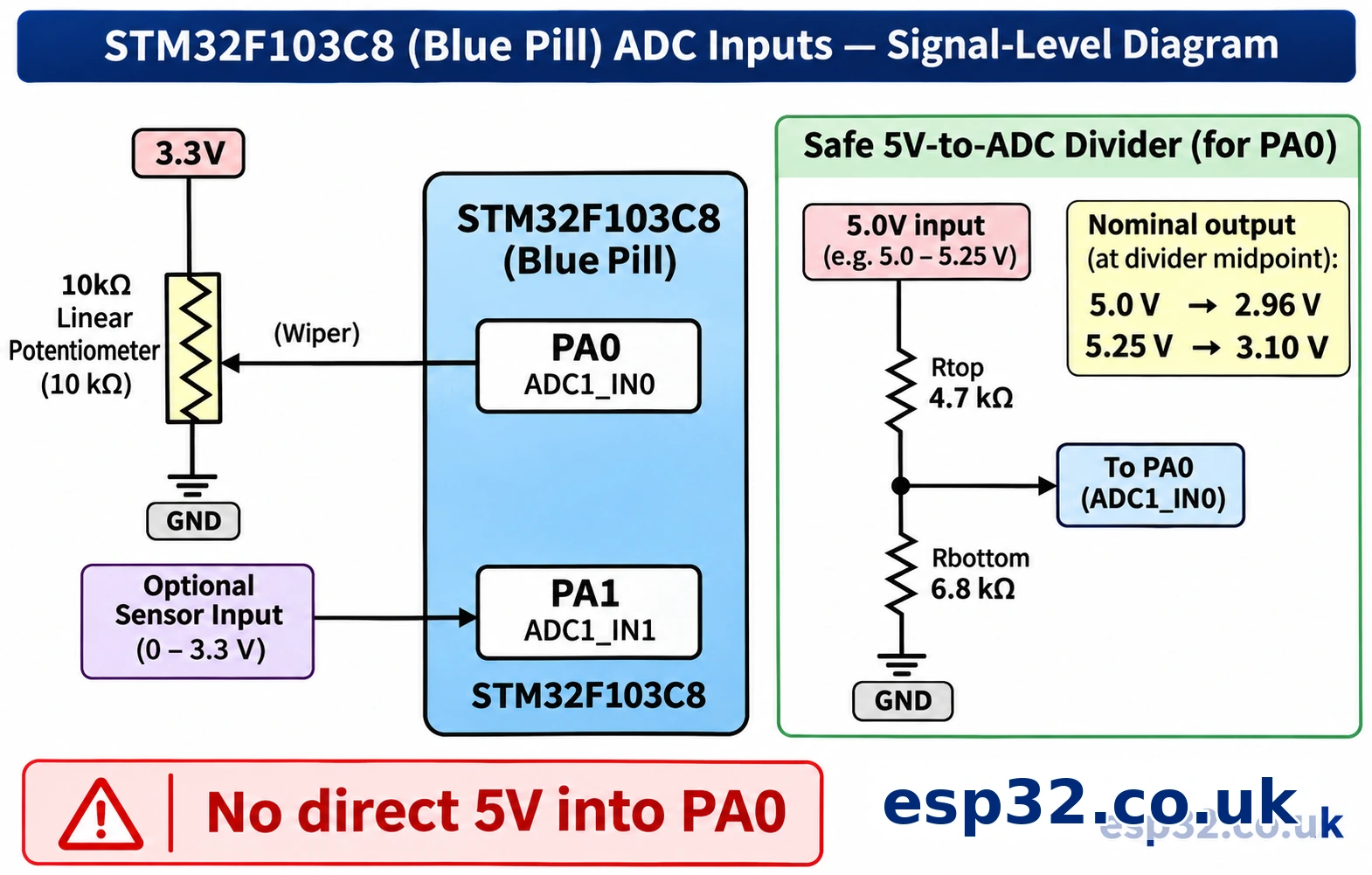
Start with a 10 kΩ linear potentiometer. Connect one outer terminal to verified 3.3 V, the other outer terminal to GND, and the centre wiper to PA0 / ADC1_IN0. This produces a variable analog voltage from approximately 0 to 3.3 V. Common ground is essential. Do not feed the potentiometer from 5 V merely because another part of your project uses 5 V.
| Potentiometer connection | Blue Pill pin | Why |
|---|---|---|
| Outer terminal A | 3.3 V rail | Upper end of the allowed range |
| Wiper / middle terminal | PA0 | ADC1 channel 0 input |
| Outer terminal B | GND | Lower end of the range |
There is normally no need for a separate digital pull-up or pull-down on PA0: the pin must be configured as analog input. Digital input circuitry and unnecessary pulls can disturb the result. Keep wires short and away from fast-switching motor or relay leads. If a sensor has a very high output impedance, consider buffering it or increasing ADC sample time rather than assuming that any resistor value will work.
For a quick sanity test, rotate the potentiometer fully one way and confirm the ADC approaches zero; rotate fully the other way and confirm it approaches 4095. Because potentiometers have tolerances, wiring resistance and end-stop behaviour, do not demand an exact 0 or 4095 under all conditions. The meaningful test is a smooth, mostly monotonic response.
Configure STM32CubeMX for ADC1 channel 0
Create a project for STM32F103C8Tx, or select the exact MCU marking and package on your board. In System Core → SYS, enable Serial Wire debug, leaving PA13 and PA14 assigned to SWD. This keeps ST-LINK programming available while you experiment with ADC settings.
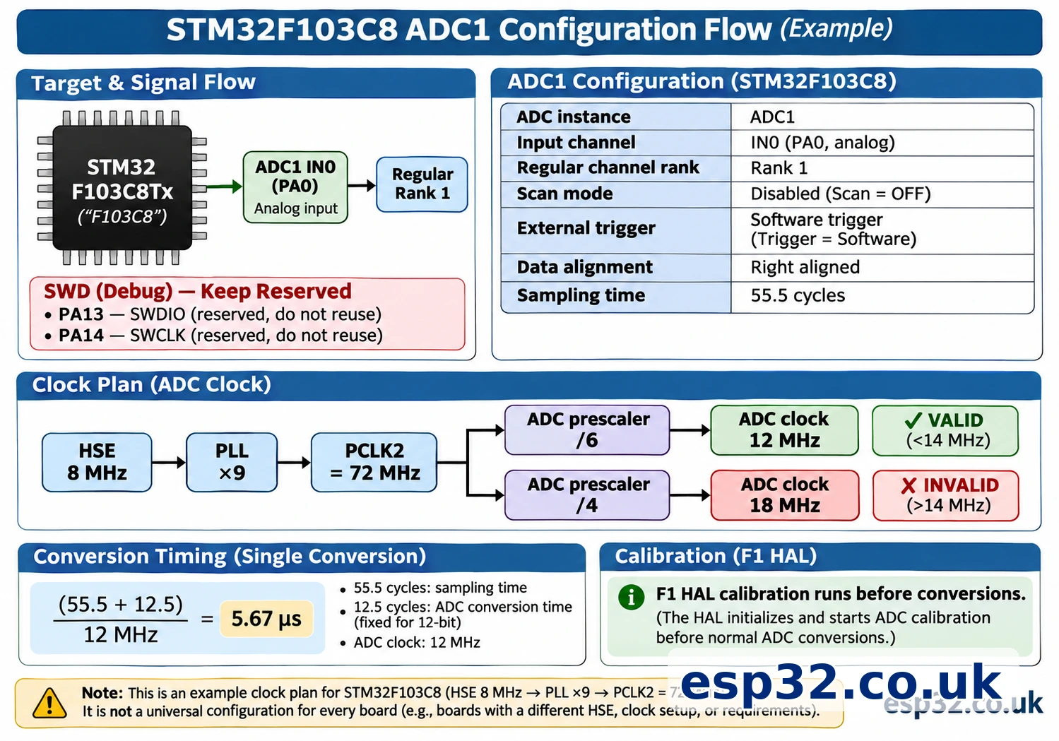
Under ADC1, select regular channel IN0. In the pinout, PA0 becomes ADC1_IN0. Set the regular conversion sequence to one rank, choose software start for this first example, right-align the data, and turn off continuous conversion. Choose a reasonable sampling period, such as 55.5 cycles initially. With a 10 kΩ potentiometer the exact required acquisition time depends on the effective source impedance and electrical conditions, but starting with a longer sample time is helpful during bring-up.
Under clock configuration, verify that the ADC prescaler yields a valid conversion clock. On a 72 MHz APB2 system, select PCLK2 / 6 = 12 MHz. Selecting PCLK2 / 4 would give 18 MHz and exceed the specified 14 MHz limit. If your project runs the CPU from an 8 MHz internal oscillator instead of a 72 MHz PLL, calculate again from the actual PCLK2—not the frequency used in another tutorial.
| CubeMX field | Single-channel polling example |
|---|---|
| MCU | STM32F103C8Tx |
| ADC instance | ADC1 |
| ADC regular channel | IN0 / PA0 |
| Rank | 1 |
| Scan mode | Disabled / not needed for one channel |
| Continuous conversion | Disabled |
| Conversion trigger | Software start |
| Data alignment | Right |
| Sample time | 55.5 ADC cycles to begin |
| ADC clock | PCLK2 divided appropriately, e.g. 72 / 6 = 12 MHz |
| NVIC / DMA | Not required for initial polling |
Generate an STM32CubeIDE project. STM32CubeIDE versions and ST project-generation workflows change over time; if CubeMX and the IDE are separate on your installation, generate code in CubeMX and import the project into CubeIDE. Inspect the generated MX_ADC1_Init() function, and confirm that ADC channel 0 and the selected sample-time setting really appear there.
Do not copy ADC code between different STM32 series without checking the HAL API and clock tree. This example is intentionally specific to the F1 family, where ADC calibration and DMA capabilities differ from newer G4, H7 or U5 parts.
First working example: read PA0 with HAL polling
Place the following code inside the appropriate user-code section of your generated main.c, after MX_GPIO_Init() and MX_ADC1_Init() have executed. The HAL headers, peripheral handle hadc1, clock setup and error handler come from CubeMX. This snippet does not replace a complete generated main.c file.
/* USER CODE BEGIN 2 */
if (HAL_ADCEx_Calibration_Start(&hadc1) != HAL_OK) {
    Error_Handler();
}
/* USER CODE END 2 */

/* USER CODE BEGIN WHILE */
while (1)
{
    uint32_t raw = 0;

    if (HAL_ADC_Start(&hadc1) != HAL_OK) {
        Error_Handler();
    }
    if (HAL_ADC_PollForConversion(&hadc1, 10) == HAL_OK) {
        raw = HAL_ADC_GetValue(&hadc1);
        /* Inspect raw in the debugger, or transmit it by UART. */
    } else {
        Error_Handler();
    }
    if (HAL_ADC_Stop(&hadc1) != HAL_OK) {
        Error_Handler();
    }

    HAL_Delay(50);
}
/* USER CODE END WHILE */
HAL_ADCEx_Calibration_Start() performs the STM32F1 calibration sequence and should run after peripheral initialization but before regular conversions begin. HAL_ADC_Start() initiates a conversion, HAL_ADC_PollForConversion() waits for completion up to the requested timeout in milliseconds, and HAL_ADC_GetValue() reads the completed result. HAL_ADC_Stop() ends the sampling cycle.
For debugging, inspect raw in STM32CubeIDE’s live expressions or pause the program after acquisition. Some debuggers show a variable only if the compiler did not optimise it away; a volatile test variable or an actual UART print path can make bring-up easier. Avoid formatting floating-point strings in a hard real-time interrupt just to observe a value.
If the ADC never completes, first verify that the ADC clock is enabled and within specification, that MX_ADC1_Init() ran, and that the regular conversion trigger is set as intended. A mismatch between software start and external timer trigger is a common reason for a timeout.
Convert the raw code into voltage and percent
Once raw ADC counts change with the potentiometer, it is tempting to display a voltage. Do this only after deciding what reference value to use. A simple helper for a known or measured reference is:
static float ADC_ToVolts(uint32_t raw, float vref_volts)
{
    if (raw > 4095U) raw = 4095U;
    return (float)raw * vref_volts / 4095.0f;
}

static float ADC_ToPercent(uint32_t raw)
{
    if (raw > 4095U) raw = 4095U;
    return 100.0f * (float)raw / 4095.0f;
}
Use ADC_ToVolts(raw, 3.30f) only if 3.30 V is a justified reference estimate. If the sensor itself is powered by 3.3 V and your application merely needs a knob position, percentage may be enough. For precision sensors, confirm the sensor output transfer function, reference measurement, calibration method and error budget separately.
At the top of the range, a 12-bit ADC saturates. A reading of 4095 cannot tell you whether the input is exactly at the reference or unlawfully above it. Clamping is not a protective circuit. Excess voltage can damage the device before firmware has the opportunity to read a code.
Why sample time matters: the input is not a perfect voltmeter
The STM32 ADC uses an internal sample-and-hold capacitor. When a channel is selected, this small capacitor must charge or discharge toward the external input voltage through the sampling switch and the sensor’s source resistance. A very short acquisition window may end before that settling is complete, especially with high-impedance sensors or when switching between channels with very different voltages.
RM0008 provides the available regular-channel sample times: 1.5, 7.5, 13.5, 28.5, 41.5, 55.5, 71.5 and 239.5 ADC clock cycles. The conversion itself requires another 12.5 ADC cycles on the F103. Therefore:
conversion time = (selected sample cycles + 12.5) / ADC clock
At a valid 12 MHz ADC clock, selecting 55.5 cycles gives (55.5 + 12.5) / 12,000,000 = 5.67 microseconds for one ideal converter operation. Choosing 239.5 cycles gives (239.5 + 12.5) / 12,000,000 = 21 microseconds. These are converter timing figures, not guaranteed sustained application sample rates: software, DMA, sequence control, trigger spacing and bus activity add constraints.
| Sample time | Total cycles including conversion | At 12 MHz ADC clock |
|---|---|---|
| 1.5 cycles | 14 | 1.17 µs |
| 7.5 cycles | 20 | 1.67 µs |
| 13.5 cycles | 26 | 2.17 µs |
| 28.5 cycles | 41 | 3.42 µs |
| 41.5 cycles | 54 | 4.50 µs |
| 55.5 cycles | 68 | 5.67 µs |
| 71.5 cycles | 84 | 7.00 µs |
| 239.5 cycles | 252 | 21.0 µs |
A longer sample time does not automatically correct all analog errors. It helps with settling but does not fix a floating input, a damaged analog rail, excessive noise or an incorrect voltage-divider ratio. The datasheet defines the maximum recommended source impedance as a function of conversion settings and tolerated acquisition error, so choose an input source and sampling time together.
Keep the ADC input within the reference range
On a 48-pin STM32F103C8, VREF+ is internally tied to VDDA, with the negative reference tied to the analog ground. This makes analog supply design crucial. A noisy 3.3 V rail produces a noisy reference. For precision measurements use an appropriate analog supply filter, local decoupling and good grounding as described in ST’s hardware design notes.
The correct analog input span is from the negative reference to VREF+. If your board exposes a 5 V power pin, this is not permission to apply 5 V to PA0. Similarly, a GPIO rated as 5 V-tolerant in digital mode does not become 5 V-tolerant while it is configured as an ADC input.
An external sensor whose signal reaches 5.0 V can be scaled with a resistor divider, provided its output can drive the divider and the design satisfies sampling impedance and accuracy requirements. For example, Rtop = 4.7 kΩ from sensor output to the sensing node and Rbottom = 6.8 kΩ from that node to ground gives:
V_PA0 = V_sensor × 6.8 / (4.7 + 6.8)
At 5.0 V input, PA0 sees approximately 2.96 V. At 5.25 V input, it sees 3.10 V. These figures assume nominal resistor values and an ideal voltage source; resistor tolerances, overvoltage transients and the sensor’s output impedance need a real design margin. Always share ground between sensor and STM32. If the sensor might experience automotive transients, reverse polarity or voltage beyond the assumed limit, add a properly rated protection/interface circuit rather than using a bare divider as a universal solution.
A divider increases the effective input impedance seen by the sample capacitor: in this example the Thevenin resistance is about 2.78 kΩ (4.7 kΩ || 6.8 kΩ), before adding any sensor impedance. It is often manageable with a suitable sample time, but calculate against the datasheet instead of assuming every fast conversion will be accurate.
Add a second analog channel: PA1 and scan mode
PA1 is ADC1_IN1. To scan PA0 and PA1 in sequence, enable ADC1 regular scan conversion, set number of conversions = 2, assign rank 1 = channel 0 (PA0) and rank 2 = channel 1 (PA1), and select suitable individual sample times. The resulting sequence is predictable: PA0, then PA1, then back to PA0 at the next trigger when scanning restarts.
A frequent mistake is to enable two GPIO analog pins but leave the ADC sequence configured for one conversion. Another is to change the rank while assuming DMA will sort the result automatically. DMA copies data in the order the ADC produces it. You must document that order in the code so the buffer indices mean what you expect.
For more deterministic sampling—such as collecting audio envelopes, current/voltage pairs or motor-control telemetry—consider a timer trigger rather than unpaced software loops. Set a trigger frequency that gives the entire ADC sequence time to complete; when two channels each take 68 ADC cycles at 12 MHz, their converter work takes roughly 11.3 µs before other timing overhead. A 1 kHz timer trigger is comfortably slower than that converter workload; it is not proof that any higher timer frequency is safe.
DMA on the F103: what it does and does not do
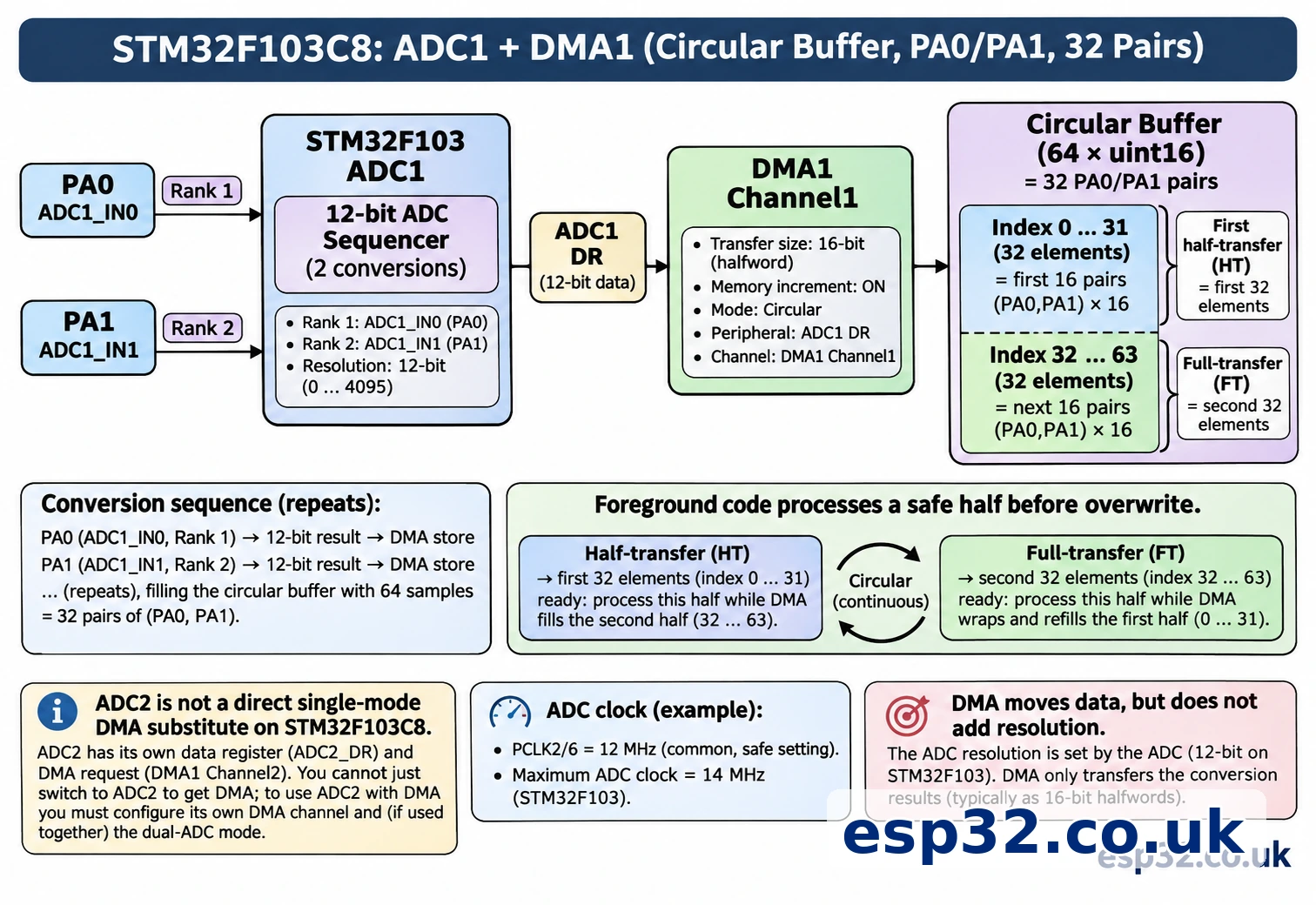
DMA moves completed ADC data into memory with less CPU involvement. On the F103C8, the usual independent regular-conversion setup uses ADC1 and DMA1 Channel1. For ordinary 12-bit samples, configure half-word (16-bit) peripheral and memory transfer sizes, peripheral-to-memory direction, and memory increment. In a multichannel scan, ADC1 presents each conversion result in sequence, and DMA stores one value per element.
DMA is a data mover, not a faster or higher-resolution ADC. It does not fix voltage-range errors, reference instability or inadequate sample time. It also does not guarantee coherent application processing if your main loop reads a buffer while DMA is overwriting it. Choose normal mode for a finite acquisition or circular mode for continuous sampling and design your buffer ownership carefully.
| Capture method | How it runs | Good first use | Main limitation |
|---|---|---|---|
| HAL polling | CPU starts and waits for each conversion | One knob or slow sensor | Foreground blocks during wait |
| ADC interrupt | ADC completion invokes callback | Infrequent event-driven conversion | IRQ overhead at higher sample rates |
| DMA normal | Finite scan fills a buffer once | Sample N readings, then analyse | Must rearm for next acquisition |
| DMA circular | Repeated ADC results overwrite ring-style buffer | Repeated sensor streaming | Must prevent processing partially overwritten data |
| Timer-triggered ADC + DMA | Hardware trigger defines conversion cadence | Repeatable sampling intervals | Trigger rate and total scan time must be compatible |
Working two-channel ADC1 DMA example
This example assumes STM32CubeMX has generated ADC1 scan mode with PA0/PA1, two ranks, continuous conversion enabled and DMA1 Channel1 in circular mode. The DMA transfer sizes must be 16 bits. Keep the hadc1 handle, ADC initialization and DMA linkage generated by CubeMX. The snippet below shows the application logic, not a complete project you can paste into a blank .c file.
/* USER CODE BEGIN PV */
static uint16_t adc_samples[2];       /* [0] = PA0, [1] = PA1 */
static volatile uint8_t adc_frame_ready = 0;
/* USER CODE END PV */

/* USER CODE BEGIN 2 */
if (HAL_ADCEx_Calibration_Start(&hadc1) != HAL_OK) {
    Error_Handler();
}
if (HAL_ADC_Start_DMA(&hadc1,
                      (uint32_t *)adc_samples,
                      2U) != HAL_OK) {
    Error_Handler();
}
/* USER CODE END 2 */

/* USER CODE BEGIN 4 */
void HAL_ADC_ConvCpltCallback(ADC_HandleTypeDef *hadc)
{
    if (hadc->Instance == ADC1) {
        adc_frame_ready = 1U;
    }
}
/* USER CODE END 4 */
With only two words in a circular buffer, DMA may start overwriting PA0 while the main loop is still reading PA1. A ready flag is only notification, not a guarantee that both reads represent the same scan. This minimal example is useful for checking the peripheral path in a debugger, but it should not be presented as a lossless or atomic acquisition system. For production measurements, use a buffer containing many complete PA0/PA1 pairs and process its half-transfer and full-transfer segments, or use a hardware timer with sufficiently separated normal-mode acquisitions. Protect against dropped segments when the consumer is slower than the producer.
For example, a 64-element circular buffer can hold 32 pairs. A half-transfer callback marks the first 32 elements (16 complete pairs) ready and a transfer-complete callback marks the second 32 elements ready. Process the indicated half before DMA returns to overwrite it. Use flags or a small event queue, avoid expensive formatting inside callbacks, and detect an overrun if the application misses a segment.
/* Conceptual addition with adc_samples[64] and circular DMA */
static volatile uint32_t adc_half_events = 0;
static volatile uint32_t adc_full_events = 0;

void HAL_ADC_ConvHalfCpltCallback(ADC_HandleTypeDef *hadc)
{
    if (hadc->Instance == ADC1) adc_half_events++;
}

void HAL_ADC_ConvCpltCallback(ADC_HandleTypeDef *hadc)
{
    if (hadc->Instance == ADC1) adc_full_events++;
}
The incrementing counters make missed notifications easier to diagnose, but they are not a complete concurrency-safe queue. Inspect and consume counters carefully in main-loop code, with interrupt masking or an appropriate critical section where needed; do not reset a counter blindly while an IRQ can increment it. For continuous high-rate signals, design the acquisition and processing pipeline around a measured worst-case processing time.
Set a meaningful sampling rate using a timer
Without a hardware trigger, “continuous conversion” means the ADC runs as fast as its configuration and peripheral allow. That may be useful for bandwidth tests but is rarely the same as “sample the sensor every millisecond.” A timer-triggered design gives reproducible intervals so you can reason about filtering, frequency content and data transfer.
A timer can produce a trigger-output event (TRGO) at a configured rate. In CubeMX, select a trigger source supported by the STM32F103 ADC1 regular group and ensure the timer’s update or compare event actually matches that ADC external-trigger selection. Then disable arbitrary software retriggering as appropriate for the configuration. A 1 kHz TRGO with a PA0/PA1 scan yields about 1,000 samples per second per channel, assuming the sequence completes before the next event and no triggers are lost.
Not every timer channel maps to every ADC trigger on F103. Consult the RM0008 trigger-selection table and the generated ADC_EXTERNALTRIGCONV_... constant. A plausible-looking but unsupported trigger selection can leave the ADC idle. Measure the conversion-ready cadence with a GPIO toggle or timer capture, not only with a debug watch window.
At 1 kHz, DMA gives the CPU most of the millisecond for other tasks. At 100 kHz, the total per-trigger budget is 10 microseconds; if your two-channel sequence itself needs 11.3 microseconds at the chosen sample time, that combination cannot finish each sequence before the next trigger. Raising the CPU MHz does not change that ADC conversion-time arithmetic when the ADC clock and sample settings stay the same.
Calibrate the ADC correctly
Calibration on STM32F1 is a hardware-assisted step intended to reduce certain converter errors. Call HAL_ADCEx_Calibration_Start(&hadc1) after ADC initialization and before the first conversions. The HAL driver handles the required F1 sequence, including converter state and timing prerequisites. If it returns an error, treat that as a problem to investigate rather than silently continuing with measurements.
Calibration is recommended after power-up, but it is not a substitute for a stable reference or an external voltage standard. It cannot know the calibration curve of your sensor, remove ground potential differences or compensate for a badly selected voltage divider. If the board warms substantially or precision is important, evaluate error over the actual operating temperature, reference tolerance and input range.
Also remember that ADC1 and ADC2 are distinct peripherals. If you use both, their configuration and calibration must be treated deliberately. The DMA example in this article uses only ADC1. Multimode ADC arrangements have additional data-format rules; do not assume that replacing hadc1 with hadc2 will preserve this DMA setup.
Improve noisy readings without hiding hardware faults
It is normal for a low-cost development board to show some ADC code variation. The right fix depends on the cause. Before adding software smoothing, measure the analog supply, confirm a defined input voltage and check whether the signal changes when USB power, a relay or a motor is activated.
For a slowly changing knob, an arithmetic moving average is an easy first filter. Averaging sixteen samples reduces uncorrelated zero-mean noise but also delays real changes; it does not remove an ADC reference offset or a periodic source of interference that is synchronous with sampling.
uint32_t sum = 0;
for (unsigned i = 0; i < 16U; i++) {
    if (HAL_ADC_Start(&hadc1) != HAL_OK) Error_Handler();
    if (HAL_ADC_PollForConversion(&hadc1, 10U) != HAL_OK)
        Error_Handler();
    sum += HAL_ADC_GetValue(&hadc1);
    if (HAL_ADC_Stop(&hadc1) != HAL_OK) Error_Handler();
}
uint16_t average = (uint16_t)((sum + 8U) / 16U);
The code above assumes a one-channel software-triggered ADC configured like the polling example, not a DMA stream already running. Do not run two competing acquisition modes on the same ADC simultaneously. To reduce noise physically, use short signal and ground paths, clean analog power, appropriate sensor buffering and an ADC sample time suited to the source. An RC filter can reduce noise, but its component values must also allow the input to settle for your intended sample rate.
For multi-channel systems, changing rank can leave traces of the previous channel if the source impedance is too large and the acquisition time too short. One diagnostic is to drive one channel near ground and the next near 3.3 V, then increase sample time and see whether the second result converges. That can reveal acquisition settling issues, but test voltages must stay within the allowed analog reference rails.
Common ADC problems and their likely causes
| Symptom | First checks | Typical correction |
|---|---|---|
| Always reads zero | PA0 wire, ground, rank 1 channel 0, analog-mode configuration | Correct wiring and generated channel setting |
| Always reads 4095 | Input near reference, wrong sensor supply, floating input | Measure actual PA0 voltage; never apply 5 V |
| HAL polling times out | ADC clock, software/external trigger mismatch, ADC initialization | Verify clock and regular trigger configuration |
| Values change with USB cable | Noisy analog reference, supply grounding | Check VDDA/VSSA, decoupling and measurement reference |
| ADC varies by hundreds of counts | Floating input, motor interference, high impedance, too-short sample time | Define/buffer input, extend sample time, fix wiring |
| DMA reports only PA0 | Scan mode/rank count or DMA length incorrect | Configure two ranks and two half-word destinations |
| DMA values swap positions | Channel ranking different from application assumptions | Review ADC sequencer rank order |
| DMA buffer never changes | DMA1 clock/linkage, IRQ, trigger or transfer sizes | Verify CubeMX DMA configuration and ADC start status |
| Clock configuration seems correct but ADC is unstable | ADC divider gives more than 14 MHz | Recalculate PCLK2/prescaler; e.g. 72/6 = 12 MHz |
| Voltage display is systematically wrong | Firmware assumes 3.300 V without measuring reference | Use measured VDDA or calibrated reference strategy |

When debugging, work in a fixed order: measure the physical voltage at the pin, confirm analog reference and ground, verify channel/rank settings, read raw 0–4095 data, and only then interpret converted volts. Changing filters and calibration constants before proving the raw input path can conceal the underlying issue.
When to use an external ADC instead
The F103 ADC is extremely useful for control knobs, battery and supply monitoring with a suitable front end, slow sensors, hobby instruments and many control loops. It is not automatically the best tool for precision thermocouple measurement, high-resolution industrial pressure sensing, isolated mains measurements or low-noise audio capture.
Consider an external ADC when you need a better characterised reference, differential inputs, higher nominal resolution, built-in programmable gain or galvanic isolation. Devices such as an ADS1115 or ADS1256 solve different problems at different sample rates and costs; higher bit count does not guarantee system accuracy. Analyse sensor noise, bandwidth, reference stability, input common-mode range and interface throughput before selecting one.
An external ADC can also free MCU pins or simplify analog front-end layout. But for simple 0–3.3 V sensing, adding an I²C ADC may introduce extra conversion latency and software complexity while providing no meaningful improvement to a noisy sensor. The best choice is dictated by the measurement budget, not by the highest advertised number of bits.
Practical project examples
A potentiometer-controlled PWM dimmer reads PA0 at a modest sample rate, smooths the raw value and maps it into a timer’s duty-cycle range. The ADC reading should not drive an LED or motor directly; an STM32 timer output drives the appropriate resistor, MOSFET driver or external circuit. Be mindful that an external LED on PC13 is a poor choice because the Blue Pill’s PC13–PC15 pins have restricted drive capabilities.
A battery monitor reads a divided battery voltage. Calculate divider ratios for the highest possible fully charged, fault and transient voltages—not just the battery’s nominal voltage. The divider should not cause excessive idle drain, and its effective resistance must be compatible with ADC acquisition time. If the battery voltage may remain present while the STM32 is unpowered, add appropriate isolation/protection; a passive divider alone can back-power semiconductor inputs.
A motor-current monitor uses a shunt amplifier or isolated sensor with an output suitable for the ADC reference range. Sampling should be synchronised with PWM switching if the application needs repeatable readings. A simple random software polling loop may sample different parts of the PWM ripple and produce misleading values, even if each conversion is individually valid.
A two-axis joystick uses PA0 and PA1. Scan both channels in a documented order, apply centre-point calibration for the actual joystick, and use a dead zone to avoid movement from small residual noise. Two ADC channels still need one sampled reading each; the numeric order in the DMA buffer follows the configured scan ranks.
Related STM32 guides on esp32.co.uk/
This ADC article follows our STM32 GPIO / LED blink tutorial and the STM32 UART / HAL / DMA tutorial. The GPIO guide explains the PA0/PA1 pin-multiplexing mindset and safe first setup; the UART guide gives you a practical way to stream ADC readings to a serial terminal for analysis.
For interfacing sensors powered from 5 V, review our STM32 GPIO and 5 V tolerance articles as background. In all cases, check the exact MCU part and board wiring rather than treating a third-party Blue Pill pin diagram as authoritative.
FAQ: STM32 ADC on the Blue Pill
Is the STM32 Blue Pill ADC really 12-bit?
Yes. The STM32F103C8 has 12-bit ADC hardware, with nominal integer output codes from 0 to 4095. If an Arduino-compatible core returns a 10-bit value, check its API’s requested read resolution; that software default does not change the underlying ADC hardware. The examples in this guide use STM32 HAL directly.
Can I measure 5 V directly with PA0?
No. PA0 in analog mode is constrained by the ADC reference and electrical ratings. Scale and protect higher voltages with suitable external components. Do not infer analog tolerance from the conditional 5 V-tolerant marking of unrelated digital pins.
Is 3.3 V always the exact ADC reference?
No. On the LQFP48 F103C8, the ADC reference is connected to the analog supply VDDA. A Blue Pill commonly supplies nominal 3.3 V, but its actual voltage and noise depend on the regulator, USB supply and board layout. Measure or otherwise establish the reference when displaying absolute voltage.
Why does a reading remain stuck even though the code builds?
A successful build does not prove that ADC1 receives a trigger or that PA0 is configured correctly. Verify the physical signal at PA0, analog-mode pin configuration, rank/channel selection, ADC clock, and whether your firmware uses software start or expects an external timer trigger.
Does DMA let ADC1 sample faster than polling?
DMA reduces CPU overhead for moving samples to RAM. The conversion clock, sample-time selection and input settling still limit valid ADC throughput. It is valuable when sampling periodically or scanning several channels because it frees the CPU to process completed buffers.
Can I use ADC2 instead of ADC1 for the DMA example?
Not as a simple drop-in replacement on the STM32F103C8. The regular single-ADC DMA path used here is ADC1. ADC2 is relevant in other configurations, including multimode, with different data handling. Follow the F1 HAL and reference-manual rules for the specific mode.
How frequently should I calibrate the ADC?
Start with calibration at initialization after power-up, before conversions. Recalibration decisions beyond that depend on your application and device conditions; do not run it blindly in the middle of an active DMA conversion. The analog reference and sensor may still require independent accuracy checks.
What is the best way to sample a sensor at precisely 1 kHz?
Use a supported hardware timer trigger at 1,000 events per second, ADC scan configuration that finishes before the next trigger, and DMA for the resulting buffer. Verify the sample interval independently. A HAL_Delay(1) loop is convenient for a demo but is not a precision 1 kHz acquisition clock.
Final engineering checklist
Before calling your STM32 ADC design complete, verify these conditions on the real board: the input voltage cannot exceed the reference or supply ratings; ADC1 uses the intended channel and rank; the input impedance is suitable for the sample time; the ADC clock is within the 14 MHz limit; calibration succeeded; conversions complete at the intended trigger rate; your DMA buffer has a defined ownership strategy; and displayed voltages use a justified reference value.
The example code and figures in this esp32.co.uk/ article are engineering guidance based on ST’s published specifications, not a claim that the project has been physically bench-tested with your particular Blue Pill revision. Validate the wiring and operating envelope on your hardware, especially when a sensor or supply can produce voltages outside the STM32’s analog range.