
The MCP3008 is an eight-channel, 10-bit analogue-to-digital converter (ADC) that connects to an ESP32AliExpress price over SPI. It is a useful alternative when the ESP32AliExpress price’s own ADC input count, pin allocation or measurements are inconvenient. It is also widely used with Raspberry Pi systems that do not have native analogue inputs. If you are searching for the MCP3008 pinout, SPI wiring, a circuit schematic, reference-voltage calculation or a first Arduino example, this guide puts those answers together.
Important distinction: Microchip makes the MCP3008 IC; Adafruit sells the 16-pin DIP chip as product #856, not a universal Adafruit-branded breakout board. Blue and green MCP3008 modules sold by third parties can have differently arranged headers, extra capacitors or solderAliExpress price links. The chip pin numbering below is definitive; breakout positions must be verified against the particular board silkscreen.
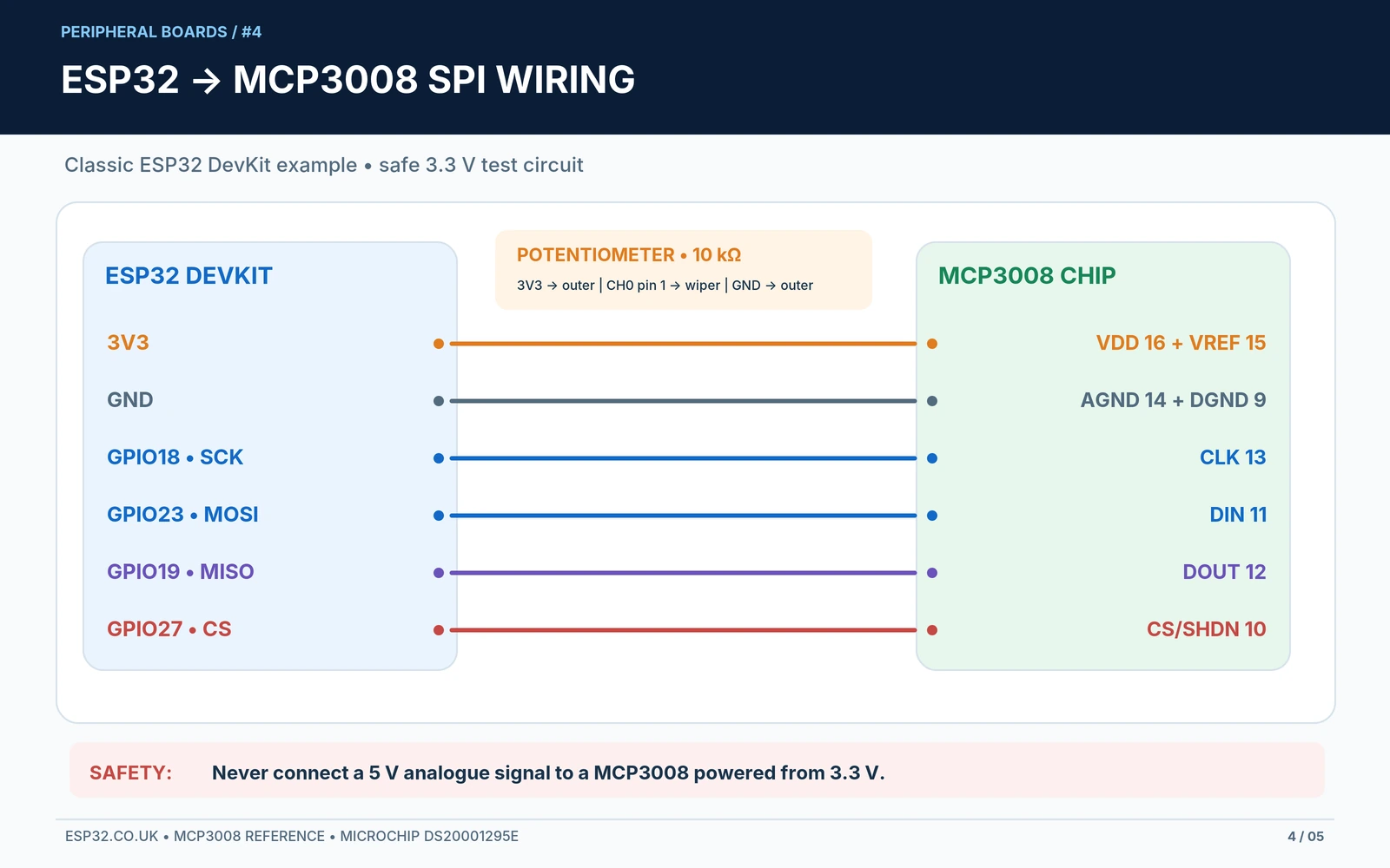
Quick wiring: for a classic ESP32 DevKit, connect the MCP3008 CLK to GPIO18, DOUT to GPIO19 (MISO), DIN to GPIO23 (MOSI), and CS/SHDN to GPIO27. Power VDD and VREF from a suitable 3.3 V rail, and connect AGND and DGND to ground. A potentiometer between 3.3 V and ground can feed CH0 safely. No I²C address, SDA, SCL or I²C solder jumpers exist on the MCP3008.
MCP3008 at a glance: specifications that matter
| Specification | What it means in practice |
|---|---|
| ADC channels | 8 single-ended channels CH0–CH7, or 4 pseudo-differential pairs |
| Resolution | 10 bits (0–1023 codes), 1024 nominal steps |
| Host connection | 4 signal wires for SPI: SCLK, MOSI, MISO and CS; plus power/reference/ground |
| Chip operating supply | 2.7–5.5 V, according to the Microchip datasheet |
| ESP32-compatible supply | Power the ADC at 3.3 V for direct 3.3 V digital SPI |
| Maximum sampling | Up to 200 kSPS at VDD=5 V; about 130 kSPS specified at 3.3 V under datasheet conditions |
| Reference input | VREF sets full-scale conversion; normally tie to clean 3.3 V for a first ESP32 project |
| SPI clock mode | Mode 0 (CPOL=0, CPHA=0), or the datasheet-supported mode 3 |
| Input limits | Normal single-ended measurement between AGND and VREF, with all electrical pins within supply limits |
| I²C address pins | None; use a separate CS signal for each chip |
| Arduino software | Adafruit MCP3008 library with Adafruit BusIO and built-in SPI |
The high advertised sampling rate is a chip capability under defined supply and clock conditions, not a promise that a loop printing every reading to Serial Monitor will reach 130,000 samples/second. SPI transactions, software scheduling, channel switching, source impedance and serial output all affect achieved throughput. At 3.3 V, start with conservative wiring, short leads and a moderate SPI clock before measuring the actual performance of your application.
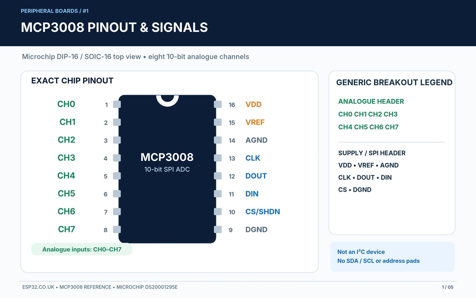
MCP3008 16-pin DIP/SOIC pinout — exact Microchip mapping
The notch or pin-1 dot establishes chip orientation. Viewed from above with the notch at the top, pins 1–8 descend down the left; pins 9–16 ascend from the bottom right. The MCP3008 is 16-pin while the related MCP3004 is 14-pin with four input channels. Do not reuse a 14-pin MCP3004 drawing.
| Chip pin | Signal | Function / connection |
|---|---|---|
| 1 | CH0 | Analogue channel 0; potentiometer wiper in example |
| 2 | CH1 | Analogue channel 1 |
| 3 | CH2 | Analogue channel 2 |
| 4 | CH3 | Analogue channel 3 |
| 5 | CH4 | Analogue channel 4 |
| 6 | CH5 | Analogue channel 5 |
| 7 | CH6 | Analogue channel 6 |
| 8 | CH7 | Analogue channel 7 |
| 9 | DGND | Digital ground: common 0 V |
| 10 | CS/SHDN | Active-low SPI chip select; HIGH deselects and enters low-power standby |
| 11 | DIN | Data INTO the ADC: connect to ESP32 MOSI |
| 12 | DOUT | Data OUT of the ADC: connect to ESP32 MISO |
| 13 | CLK | SPI serial clock: connect to ESP32 SCK |
| 14 | AGND | Analogue ground: clean common 0 V reference |
| 15 | VREF | Analogue reference, e.g. 3.3 V; sets full-scale span |
| 16 | VDD | ADC power supply; 3.3 V for example |
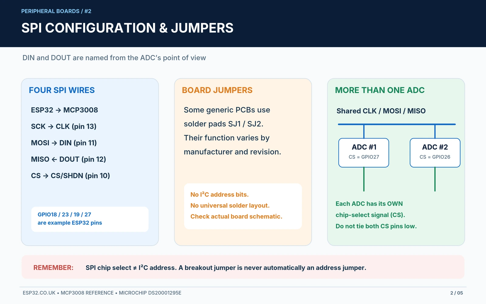
DIN and DOUT are named from the ADC’s point of view: MCP3008 DIN receives the ESP32’s MOSI; MCP3008 DOUT drives the ESP32’s MISO. Swapping these two wires is one of the most common causes of all-zero or invalid readings. CH0…CH7 are analogue inputs, not GPIO outputs.
MCP3008 breakout boards and jumpers: what can be configured?
Some modules bring all 16 MCP3008 pins to labelled headers; others group CH0–CH7 on one edge and VDD, VREF, AGND, CLK, DOUT, DIN, CS, DGND on another. Some seller images show pads marked SJ1 and SJ2. They are not a universal standard. On an individual PCB, a link might join VREF to VDD or common a pair of ground nets; the only safe way to identify the function is the maker’s schematic or PCB continuity test. Never assume a solder jumper changes an I²C address — there is no I²C interface on this IC.
If your module contains a reference-voltage trimmer, external reference header or other circuitry, its analogue behaviour is board-dependent. A basic DIP-16 MCP3008 in a breadboard has no address or configuration jumpers; the selected channel and single-ended/pseudo-differential mode are encoded in the SPI command sent for each reading.
Why is MCP3008 not an I²C sensor?
Unlike the ADS1115 and PCF8591 modules, the MCP3008 does not respond at an address such as 0x48. An ESP32 I²C scanner cannot discover it. Each conversion requires toggling chip select, sending a start bit and a channel configuration over MOSI, and clocking the conversion bits back over MISO. If two MCP3008 chips share SCK/MOSI/MISO, use a separate CS pin per chip.
Functional circuit schematic: reference, decoupling and ground
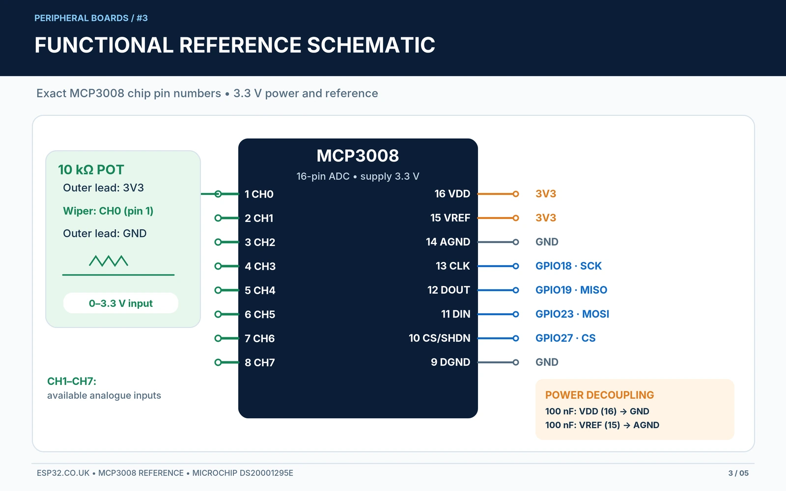
For a dependable starter circuit, connect MCP3008 VDD (pin 16) to ESP32 3V3 with a nearby 100 nF ceramic decoupling capacitor between VDD and DGND; connect VREF (pin 15) to the same clean 3.3 V rail and decouple/reference-route it appropriately. Connect AGND (pin 14) and DGND (pin 9) to a shared system ground with careful analogue return routing. Supply-voltage variations also change the calculated input voltage when VREF simply follows the supply.
The VREF input can be driven from a lower, suitably clean precision reference to obtain finer nominal voltage steps over a smaller measuring range. Microchip specifies the reference as an input from around 0.25 V to VDD, but accuracy and linearity depend on the reference voltage and analogue-source conditions. Lowering VREF does not make higher voltages safe on input pins. Keep every analogue and digital signal within its permitted pin limits.
Do not confuse reference voltage with ADC supply voltage. For example, VDD can remain 3.3 V while a valid independent precision VREF defines the input conversion span. Also, an input divider lets you observe a higher external voltage only when carefully designed to keep the MCP3008 pin within limits, with sensible grounding, resistor tolerances and expected fault voltages. Do not connect a 5 V sensor directly to CH0 when the ADC is powered from 3.3 V.
ESP32 to MCP3008 wiring: complete 3.3 V SPI example
| Classic ESP32 DevKit | MCP3008 | Purpose |
|---|---|---|
| 3V3 | VDD (pin 16) | 3.3 V converter supply |
| 3V3 | VREF (pin 15) | Nominal 3.3 V reference |
| GND | AGND (pin 14) | Analogue ground reference |
| GND | DGND (pin 9) | Digital ground |
| GPIO18 (SCK) | CLK (pin 13) | SPI clock |
| GPIO23 (MOSI) | DIN (pin 11) | Microcontroller data to ADC |
| GPIO19 (MISO) | DOUT (pin 12) | ADC results to microcontroller |
| GPIO27 (CS) | CS/SHDN (pin 10) | Active-low chip select; separate GPIO per additional chip |
| Potentiometer wiper | CH0 (pin 1) | 0–3.3 V adjustable test input |
A typical 10 kΩ potentiometer test has one outside terminal on 3V3, the other outside terminal on ground, and its wiper on CH0. Varying the knob should smoothly change a CH0 reading from close to 0 to close to 1023. This setup is more reliable for an introductory example than leaving CH0 floating or applying an arbitrary unverified sensor output. Remaining channels should have defined voltages if you want stable measurements.
Why GPIO27 for CS? It is a convenient general-purpose output on many classic ESP32 DevKits. Many projects use GPIO5 for SPI CS, but GPIO5 is a classic ESP32 boot-strapping pin, so choosing GPIO27 avoids one potential boot-configuration interaction. You can use another appropriate free GPIO. ESP32-S3, C3, C6 and other families have different available GPIOs; choose their actual SPI pin mapping and amend SPI.begin().
Arduino IDE: install the Adafruit MCP3008 library
In Arduino IDE 2, use Library Manager to install Adafruit MCP3008 by Adafruit. Install its dependency Adafruit BusIO if prompted. Select an ESP32 board and upload the example below. The library API used here — begin(cs, &SPI), readADC(channel) and readADCDifference(code) — is confirmed in the public Adafruit library source. You do not need to manually bit-bang the SPI protocol for a first test.
The example explicitly initialises the classic ESP32 SPI peripheral as SCK=18, MISO=19, MOSI=23, CS=27. It reads all eight ADC channels, converts each code to an approximate voltage and prints at 115200 baud. We use VREF=3.3 V only because it was wired that way; if you connect a different measured reference, change the software value.
#include <Arduino.h>
#include <SPI.h>
#include <Adafruit_MCP3008.h>

constexpr int SPI_SCK  = 18;
constexpr int SPI_MISO = 19;
constexpr int SPI_MOSI = 23;
constexpr int ADC_CS   = 27;

constexpr float ADC_VREF = 3.300f;  // Verify actual voltage at VREF

Adafruit_MCP3008 adc;

void setup() {
  Serial.begin(115200);
  delay(500);

  SPI.begin(SPI_SCK, SPI_MISO, SPI_MOSI, ADC_CS);

  if (!adc.begin(ADC_CS, &SPI)) {
    Serial.println("SPI device initialization failed");
    while (true) delay(1000);
  }

  // SPI has no device-acknowledgement stage.
  // A successful begin() does not prove the MCP3008 is wired.
  Serial.println("MCP3008: reading CH0-CH7");
}

void loop() {
  for (uint8_t channel = 0; channel < 8; ++channel) {
    int16_t raw = adc.readADC(channel);
    if (raw < 0) {
      Serial.printf("CH%u: invalid\t", channel);
      continue;
    }

    // 10-bit ADC has 1024 quantisation intervals.
    float volts = raw * (ADC_VREF / 1024.0f);
    Serial.printf("CH%u: %4d (~%.3f V)  ", channel, raw, volts);
  }
  Serial.println();
  delay(400);
}
Note on device detection: SPI has no built-in address acknowledgement like I²C. The library’s begin() tells you whether it could initialise its SPI helper, not whether a real MCP3008 answered. With the chip missing or DOUT disconnected, you may still see apparently valid numerical outputs — often zero or a fixed pattern. Test with a known low/mid/high input voltage or use an oscilloscope to verify CS, CLK and DOUT.
Example serial output
MCP3008: reading CH0-CH7
CH0:  511 (~1.647 V)  CH1:    0 (~0.000 V)  CH2: 1023 (~3.297 V) ...
CH0:  647 (~2.085 V)  CH1:    0 (~0.000 V)  CH2: 1023 (~3.297 V) ...
The numbers above are illustrative; they are not laboratory test results and do not imply an unconnected input should report a fixed number. You must deliberately connect each sensor channel to a valid analogue signal for meaningful values.
Understanding resolution, reference voltage and the 0–1023 scale
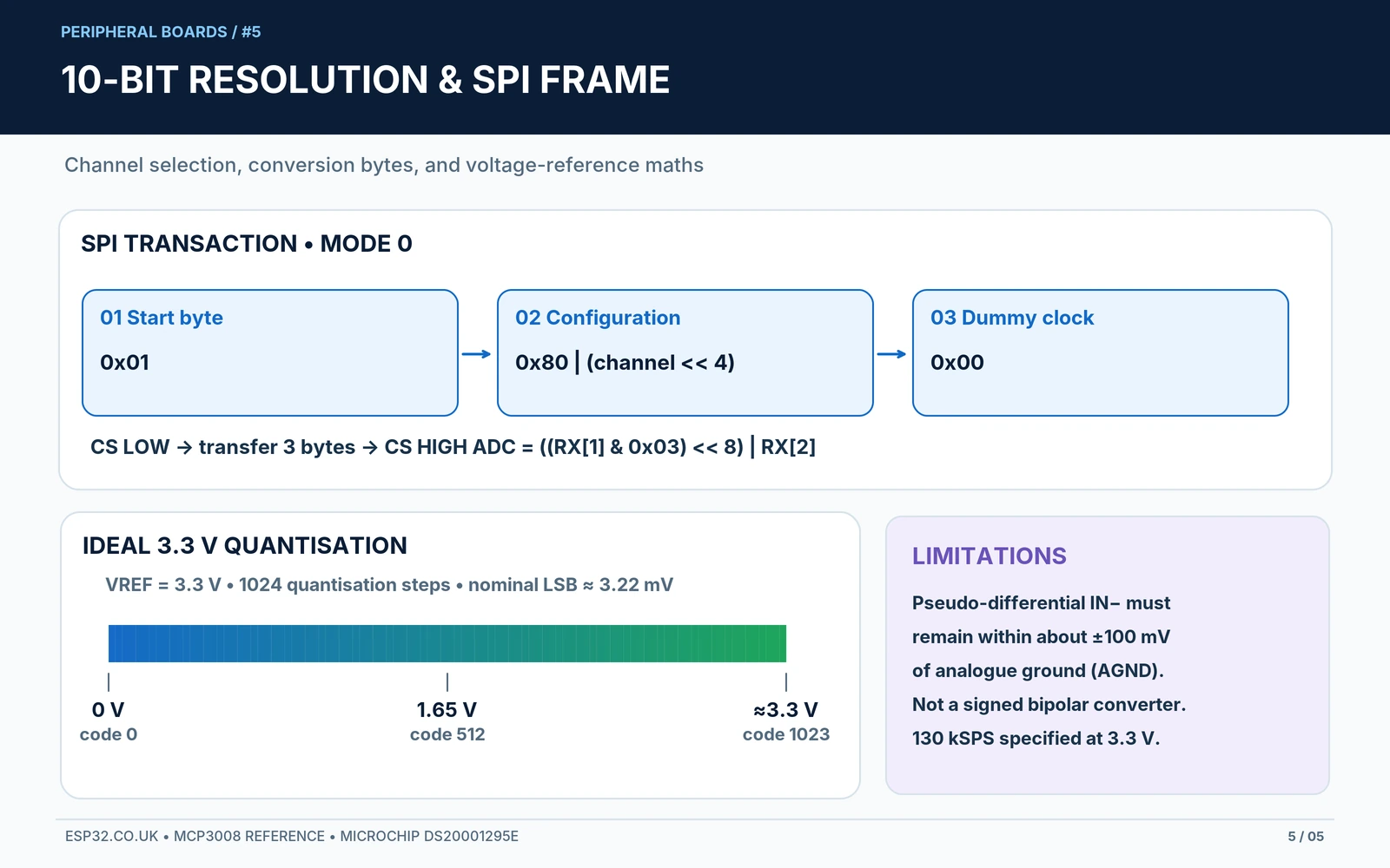
For a single-ended measurement, the ideal code is approximately floor(1024 × VIN / VREF), clipped to 0–1023. With a 3.3 V reference, each least-significant bit (LSB) represents about 3.22 mV. An ADC reading is a quantised estimate of a voltage, not a precision voltmeter unless the reference, source impedance, layout and input errors are under control.
| Nominal CH0 input | Expected ideal code (approx.) | Estimated voltage from code |
|---|---|---|
| 0 V | 0 | 0.000 V |
| 0.825 V | 256 | 0.825 V |
| 1.650 V | 512 | 1.650 V |
| 2.475 V | 768 | 2.475 V |
| Just below 3.3 V | 1023 | 3.297 V (largest code estimate) |
Notice that dividing by 1023 puts the highest code exactly at the nominal reference, but Microchip’s ideal quantisation relationship uses 1024 steps. For simple approximate voltage output the code above uses 1024.0. Full-scale saturation and real hardware error mean a reading of 1023 does not uniquely identify an exact input voltage.
SPI configuration and byte sequence: why no I²C address?
A typical single-ended MCP3008 read uses SPI mode 0 with a chip-select-low transaction. It sends 0x01 (start), then (0x08 | channel) << 4 (single-ended selection and three channel bits), then an extra byte to clock out the remaining conversion bits. The ADC’s ten result bits are extracted from the final received bytes. The Adafruit library hides this transfer logic, which is convenient for applications.
// Protocol reference only: illustrative raw SPI transaction.
// The Adafruit library already implements this.
int readChannelRaw(uint8_t channel) {
  if (channel > 7) return -1;

  SPI.beginTransaction(SPISettings(1000000, MSBFIRST, SPI_MODE0));
  digitalWrite(ADC_CS, LOW);
  SPI.transfer(0x01);                 // Start bit
  uint8_t hi = SPI.transfer((0x08 | channel) << 4);
  uint8_t lo = SPI.transfer(0x00);
  digitalWrite(ADC_CS, HIGH);
  SPI.endTransaction();

  return ((hi & 0x03) << 8) | lo;      // 10-bit result
}
The raw example assumes ADC_CS is configured as an output and driven HIGH before the first call; the earlier library sketch configures the pin through its SPI helper. Do not paste this function into an unrelated project without setting up SPI, CS and transaction ownership. The register-free serial protocol is straightforward, but correct clock polarity, timing and CS edges still matter.
Pseudo-differential mode: what it can and cannot measure
The MCP3008 can interpret channel pairs (CH0/CH1, CH2/CH3, CH4/CH5 and CH6/CH7) as pseudo-differential inputs using the appropriate command bits. The selectable polarity allows either channel in the pair to act as IN+. However, this does not mean it can measure an arbitrary positive or negative differential signal: Microchip specifies IN− close to ground (approximately within ±100 mV of AGND). The output is a nonnegative straight-binary code clipped at zero, not a signed bipolar voltage measurement.
The Adafruit library exposes readADCDifference(code) for code values 0–7, corresponding to the eight polarity choices across four adjacent channel pairs. A result should only be interpreted using the datasheet’s allowed input-common-mode range and reference relationship. For true differential measurements at elevated common-mode voltage or for substantially better resolution, consider a purpose-designed instrumentation front end or a different ADC such as the ADS1115, while still observing its pin voltage limits.
How to choose an external ADC: MCP3008 versus ADS1015 and ADS1115
| Feature | MCP3008 | ADS1015 | ADS1115 |
|---|---|---|---|
| Host bus | SPI | I²C | I²C |
| Channels | 8 single-ended | 4 single-ended | 4 single-ended |
| Resolution | 10-bit | 12-bit | 16-bit |
| Max nominal conversion rate | Up to 200 kSPS at 5 V | 3,300 SPS | 860 SPS |
| Typical use | More fast-ish simple channels, SPI devices | Four channels with speed | Four channels with higher resolution |
These are simplified feature comparisons rather than guaranteed board-level accuracy or sustained application rates. The MCP3008’s speed and channel count are attractive for multiplexed knobs and simple sensor arrays. For slower measurements where the number of volts per code matters more, see the site’s ADS1115 with ESP32 guide and the ADS1115 breakout pinout reference.
Troubleshooting: common MCP3008 errors
| Symptom | Likely cause and fix |
|---|---|
| All channels read zero | Check ADC VDD, both grounds, CS activity, correct MISO from MCP3008 DOUT, and a known powered input. |
| Every channel shows the same value | Channel-selection bits wrong, input multiplexing issue or floating inputs; verify CH0–CH7 connection. |
| I²C scanner sees no MCP3008 | Expected: it is an SPI device without an I²C address. |
| ADC input appears capped or damaged | Sensor voltage above permitted pin/supply limits. Do not feed 5 V to a 3.3 V MCP3008. |
| Reading unstable with 100 kΩ potentiometer | Sampling capacitor and high source impedance; use a lower-impedance source such as 10 kΩ and decouple correctly. |
| ESP32 does not boot | Check whether CS was placed on a strapping pin. GPIO27 is used here to avoid the common GPIO5 strap. |
| Wrong voltage calculation | VREF not equal to assumed 3.3 V, poor reference or incorrect 1024-step conversion. Measure the reference. |
| SPI responds but waveform is distorted | Incorrect polarity/phase, overly high SPI frequency, long cables or unstable supplies. Start at SPI mode 0. |
| MISO and MOSI seem reversed | MCP3008 DIN connects to ESP32 MOSI; MCP3008 DOUT connects to ESP32 MISO. |
| Differential mode returns only positive readings | Expected: MCP3008 pseudo-differential mode is ground-referenced and unsigned; it is not a signed bipolar ADC. |
MCP3008 FAQ
Does the MCP3008 have an I²C address or selectable solder-address pads?
No. It uses four SPI signal lines and a dedicated CS/SHDN pin. Breakout-board solder links, when present, may relate to the reference supply or board wiring and are not standardised I²C address controls.
Can MCP3008 read 5 V sensors on an ESP32?
Not directly when powered at 3.3 V. A suitable divider or analogue front end may be needed to keep the voltage at the ADC pin in its operating range, including transients. Always check the board’s real reference and supply.
Is MCP3008 better than the ESP32 ADC?
It offers eight independent external analogue inputs with a defined external reference and a separate SPI interface. Whether it is better depends on measurement noise, calibration, required resolution, routing, sampling speed and the ESP32 variant. It is not automatically more accurate in every circuit.
Can I connect two MCP3008 chips to the same ESP32?
Yes. Share SCK, MOSI and MISO with separate chip-select lines, then initialise a separate library object for each CS. Ensure that the two chips are deselected when they are not being addressed, and keep power/ground/reference wiring sound.
Why does the example use a different CS GPIO from the usual VSPI defaults?
GPIO27 is deliberately chosen on a classic ESP32 DevKit to avoid tying the ADC to the common GPIO5 boot-strap signal. SPI CS is software-selectable, so you can adapt it to another safe available pin.
Manufacturer sources and related guides
- Microchip MCP3004/MCP3008 datasheet, DS20001295E — authoritative pin mapping, differential limits, timing and reference equations.
- Microchip MCP3008 product page — in-production part information and package variants.
- Adafruit MCP3008 product #856 — bare DIP-16 IC (not a breakout PCB).
- Adafruit MCP3008 Arduino library — begin(cs, &SPI), readADC, readADCDifference, and BusIO dependency.
- Adafruit MCP3008 tutorial — accessible SPI ADC introduction.
Editorial and hardware caveat: The exact 16-pin mapping is based on the Microchip manufacturer datasheet. Example breakout photographs or diagrams are generic unless the maker and PCB revision can be identified. The Arduino example has been checked against the published library interface, but it has not been physically tested on the reader’s wiring.