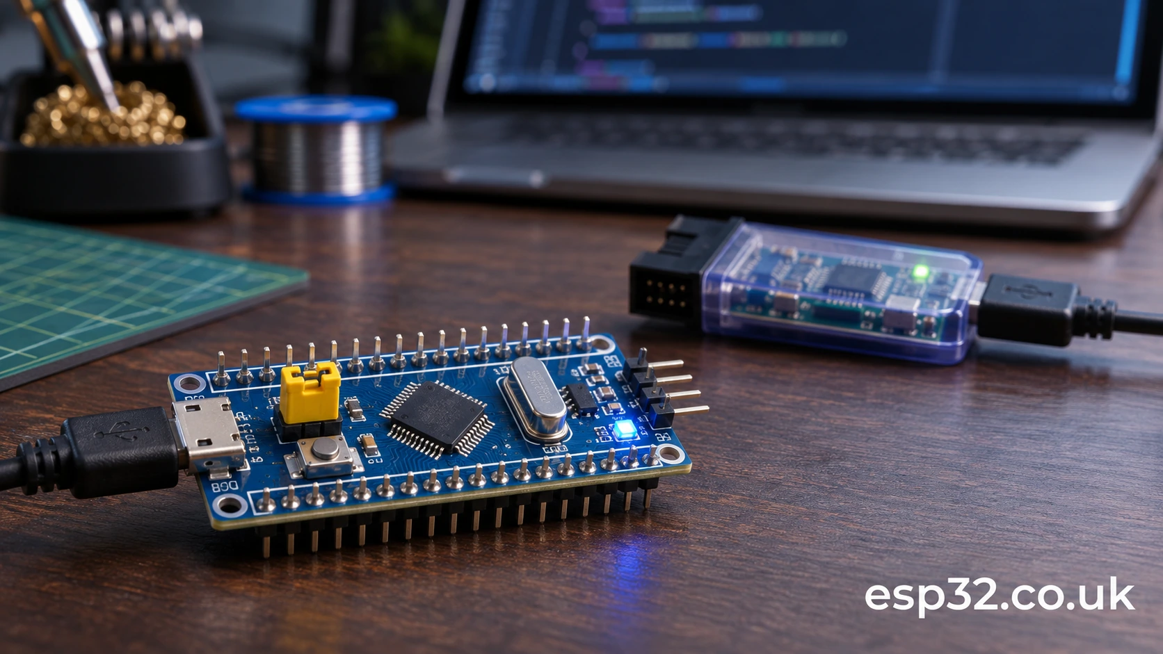
Want your first STM32PriceAliExpress price LEDPrice blink to work reliably? Configure a GPIO output in STM32CubeMX, generate an STM32CubeIDE project, and call HAL_GPIO_TogglePin() followed by HAL_Delay() inside the main loop. On a typical STM32F103C8PriceAliExpress price Blue PillAliExpress price, the built-in LED is connected to PC13 and is active-low: writing GPIO_PIN_RESET turns it on, while GPIO_PIN_SET turns it off. The simplest repeatable example uses PC13 with low-speed push-pull output and a 500 ms delay.
In this tutorial we will build that project from an empty CubeMX configuration, explain every relevant HAL call, add a separate LED on PA5, read a button on PB0, and diagnose the common problems that make a first STM32 project appear broken. The examples target the STM32F103C8T6 Blue Pill unless a board is explicitly identified otherwise. If you have a NUCLEO-F401RE or NUCLEO-F446RE, its user LED is typically PA5 and active-high—do not copy the PC13 board assumption.
Quick answer: minimum STM32 HAL blink example
For a correctly initialised STM32F103C8 project with PC13 configured as a GPIO output, this is all the application loop needs:
/* Inside while (1) in Core/Src/main.c */
while (1)
{
    HAL_GPIO_TogglePin(GPIOC, GPIO_PIN_13);
    HAL_Delay(500);
}
The initialization is not optional. MX_GPIO_Init() must enable the GPIOC peripheral clock and configure PC13 before the loop executes. HAL_Init() establishes the HAL timebase; SystemClock_Config() applies the clock choices generated by CubeMX. A correct while (1) can still show no light if the pin is in input mode, the board is unpowered, the flash operation failed, or the LED is attached to a different pin.
| Setting | Blue Pill built-in LED | External LED example |
|---|---|---|
| MCU pin | PC13 | PA5 |
| Typical LED logic | Active-low | Active-high in our circuit |
| GPIO mode | Output push-pull | Output push-pull |
| Pull-up or pull-down | No pull | No pull |
| GPIO output speed | Low, at most 2 MHz for PC13 | Low is enough for blinking |
| Hardware | LED and series resistor already on the board, verify revision | 330 Ω series resistor and LED to ground |
| Debug/program | ST-LINK via PA13 SWDIO and PA14 SWCLK | Same ST-LINK connection |
Electrical warning: PC13, PC14 and PC15 are special low-drive pins on the F103. ST specifies a maximum 3 mA output current and says these pins should not source LED current. The usual Blue Pill onboard LED works by sinking a small current when PC13 is low. Use a more capable ordinary GPIO, such as PA5 with a current-limiting resistor, for your own external LED. Never wire an LED directly across a GPIO and a supply without a resistor.
What you need before starting
This is a small, low-cost test; the important thing is to keep the programming path separate from the application circuit.
- An STM32F103C8T6 Blue Pill development board, preferably with known MCU provenance.
- A USB-connected ST-LINK debugger/programmer and suitable SWD leads, or a Nucleo board with onboard ST-LINK.
- STM32CubeMX and STM32CubeIDE installed. In CubeIDE 2.x, CubeMX is a separate project-configuration application.
- A USB data cable for ST-LINK, not a charge-only cable.
- Optionally, an LED, a 330 Ω resistor, a breadboard, a normally-open push button and short jumper wires.
- A multimeter for checking the board’s regulated 3.3 V rail and ground if programming fails.
You do not need the Blue Pill’s Micro-USB connector to run this program. The STM32F103C8 has USB device hardware, but its factory system-memory bootloader does not provide the convenient native USB DFU path offered by some other STM32 parts. ST-LINK over SWD is the most reproducible first-project route, including for boards with uncertain USB pull-up hardware.
Understand a GPIO pin before changing CubeMX settings
GPIO means general-purpose input/output. A physical MCU pad can usually be configured as a digital input, digital output, alternate-function signal or analog input, subject to the pin and device. GPIOC, pin 13 identifies the port and bit; it does not identify the 13th physical connector pin on your particular development board. In code, GPIOC is the peripheral address and GPIO_PIN_13 is the corresponding bit mask.
A digital output has two logical states. A push-pull output actively drives high or low within the MCU’s valid electrical limits. An open-drain output actively pulls low but needs an external or internal pull-up arrangement to reach a reliable high state. A digital input senses a signal; floating inputs have no guaranteed stable state. Pull-ups and pull-downs establish a defined state when no external source drives the pin.
The STM32F1 pin configuration model differs in details from newer STM32 families. CubeMX hides many register differences but the distinction matters if you later copy code between F1, F4 and G4 projects. In particular, don’t assume an F1 GPIO_InitTypeDef has every member or alternate-function field used by a later family.
| GPIO term | Meaning | Why it matters for an LED |
|---|---|---|
GPIO_MODE_OUTPUT_PP | Digital push-pull output | Directly sets high or low |
GPIO_MODE_OUTPUT_OD | Open-drain output | Requires an appropriate pull-up for a high level |
GPIO_MODE_INPUT | Digital input | Cannot drive an LED deliberately |
GPIO_PULLUP | Pull-up bias for an input | Useful for a button wired to ground |
GPIO_NOPULL | No internal input pull | Fine for push-pull LED outputs |
GPIO_SPEED_FREQ_LOW | Low output slew/speed configuration | Prefer for slow LEDs and reduced switching noise |
GPIO_PIN_SET | Output high | Off for an active-low PC13 LED |
GPIO_PIN_RESET | Output low | On for a typical active-low PC13 LED |
Think of these as hardware choices, not merely names to satisfy a compiler. A high GPIO setting does not imply the external device receives enough current, nor does a 3.3 V GPIO accept an arbitrary 5 V input. Some specified STM32F103 digital pins are five-volt tolerant under datasheet conditions, but PC13 and analog-capable pins must not be treated as universally 5 V tolerant. Use proper level shifting for mixed-voltage electronics.
Blue Pill onboard LED: why PC13 works backwards
On many common Blue Pill revisions the onboard indicator LED and its resistor are connected from the 3.3 V supply toward PC13. When PC13 outputs low, current flows through the resistor and LED into the MCU pin; the LED lights. When PC13 outputs high, little voltage remains across the LED, so it goes dark. That is the meaning of active-low.
If you begin by writing HAL_GPIO_WritePin(GPIOC, GPIO_PIN_13, GPIO_PIN_SET);, you are usually selecting LED off. The initial high level is useful because it prevents an unwanted flash during startup. Some clone boards differ, and a dead LED is possible; check your actual PCB rather than inventing a universal Blue Pill schematic.
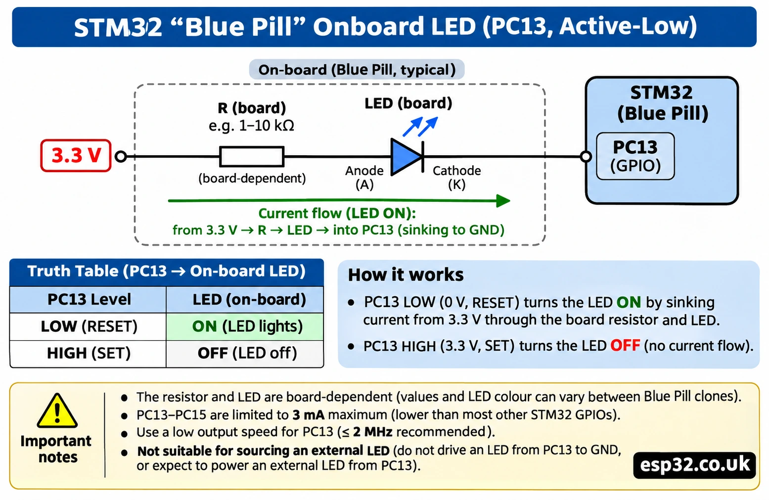
This is also why tutorials that attach an extra LED between PC13 and GND can be misleading. They reverse the expected electrical arrangement and may exceed PC13’s allowable source current. The safer second example in this guide uses PA5 with a resistor. We use PC13 only for the small onboard indicator that the board designer already provided.
Connect ST-LINK to the STM32 Blue Pill correctly
For SWD programming, connect SWDIO to PA13, SWCLK to PA14, and GND to GND. Connect the programmer’s target-voltage-sense/reference input to a verified 3.3 V target rail if the probe requires it. An optional NRST line can improve recovery when firmware reconfigures debug pins or the target is unstable. Supply target power through an intentional, compatible power source; don’t assume a pin labelled Vref is a power output.
| ST-LINK signal | Blue Pill signal | Role |
|---|---|---|
| SWDIO | PA13 | Bidirectional SWD data |
| SWCLK | PA14 | SWD clock |
| GND | GND | Common ground reference |
| VTref / TVCC sense | Verified target 3.3 V | Allows programmer to sense target voltage |
| NRST, optional | NRST | Connect-under-reset recovery |
Do not use the pin order of a cheap four-pin ST-LINK clone as a universal reference. Genuine ST-LINK/V2, STDC14-based V3 probes and clone USB dongles have different connectors. Identify signals from the label and the probe’s actual manual, not from the wire colours or a random photograph. The LED tutorial does not need SWO, UART, CAN or USB connections between the MCU and the debugger.
For normal flashing, leave BOOT0 at 0 so the MCU starts user flash after reset. SWD itself does not require BOOT0 high or a factory UART loader. A board that will only connect with reset asserted may have clock, option-byte, debug-pin, wiring or power problems; first lower the SWD frequency and try connect-under-reset rather than erasing the whole device.
Create the STM32F103C8 project in STM32CubeMX
Open STM32CubeMX and select New Project → MCU/MPU Selector. Search for the precise part STM32F103C8Tx (the suffix in CubeMX’s selector may vary from the marking on your actual chip), then confirm it is the LQFP48 part and not a larger Nucleo or F103RB target. Create a project named BluePill_GPIO_Blink with a directory you can write to.
In System Core → SYS, choose Serial Wire as the debug interface. This keeps PA13 and PA14 available for your SWD programmer instead of accidentally assigning them as ordinary GPIO. CubeMX usually exposes a visual pin view; click PC13 and select GPIO_Output. In System Core → GPIO, set PC13 to push-pull output, no pull, and low output speed. Name it LED_PC13 if you want clear symbolic constants.
Set the initial output level to High on this active-low board. This avoids starting the app with the LED on and makes the first toggle visibly turn it on. A beginner can use the internal HSI oscillator and CubeMX’s standard clock configuration. There is no need to configure a 72 MHz PLL, an external crystal, or a USB 48 MHz clock for an LED that blinks twice per second.
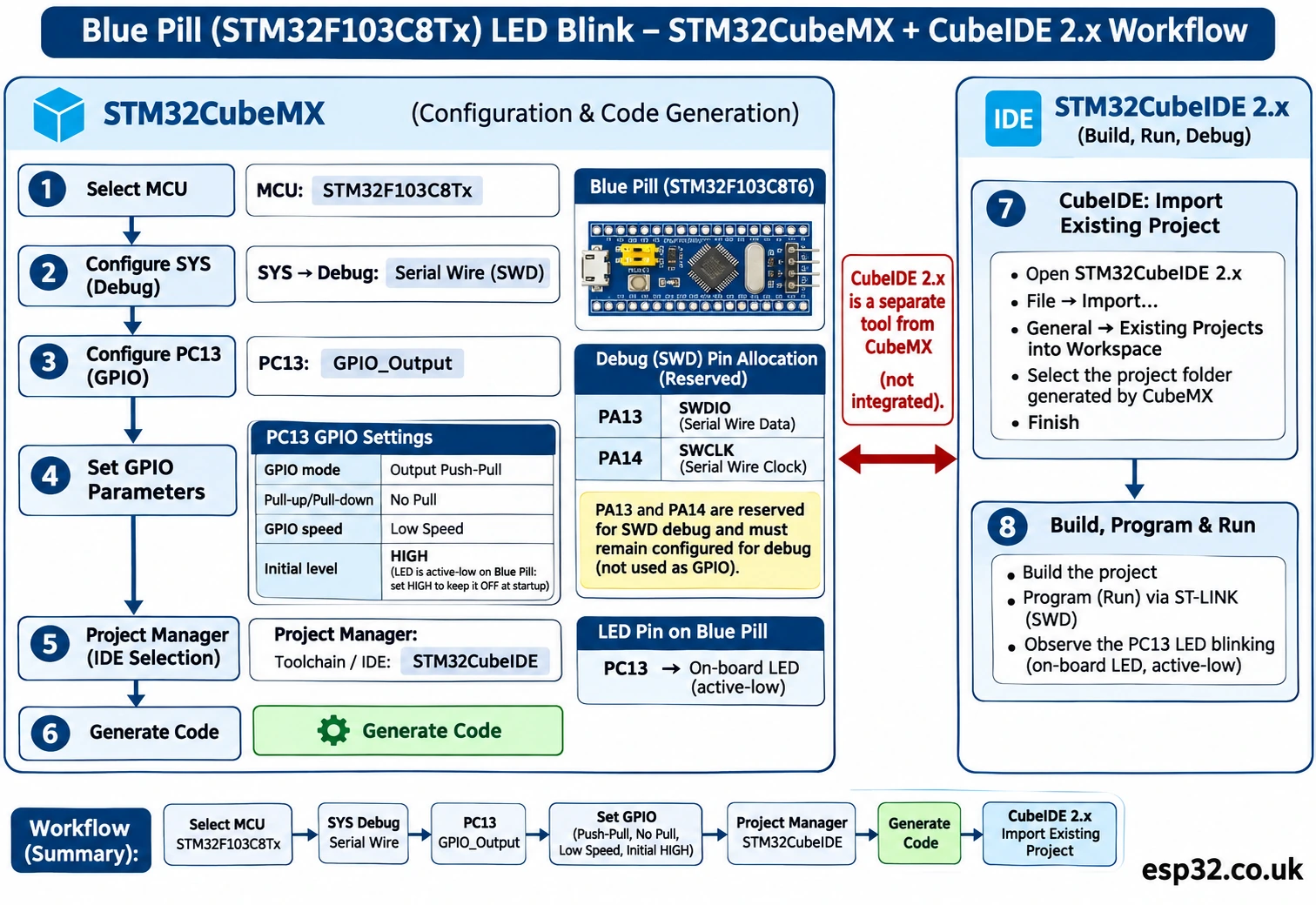
A good first project has as few moving parts as possible. CubeMX can generate higher-speed PLL projects using the board’s external 8 MHz crystal, but enabling HSE before proving the board works adds a second failure mode. If your board’s HSE oscillator is defective or has unusual capacitor values, a correct GPIO project can fail early in clock configuration. Start with HSI; add HSE and PLL only when the basic LED behavior is verified.
Generate the separate CubeIDE project
In CubeMX Project Manager, select STM32CubeIDE as the toolchain and request generated peripheral-initialization code. Download the matching STM32CubeF1 firmware package if the tool prompts you. Generate code, then open STM32CubeIDE and import the generated project using File → Import → General → Existing Projects into Workspace. Select the generated project’s root directory and import it. The exact wizard wording can change between releases, but the concept is unchanged: CubeMX generates the configuration and project; CubeIDE builds and debugs it.
Older videos show CubeMX configuration integrated directly inside an earlier CubeIDE version. The separated STM32CubeIDE 2.x workflow is not an installation error. The standalone CubeMX project .ioc remains the configuration source and CubeIDE remains the C/C++ build and debug environment. Save the .ioc alongside your project rather than treating it as a disposable file.
Where to put your application code
Open Core/Src/main.c. The generated file normally calls HAL_Init(), SystemClock_Config(), MX_GPIO_Init() and then enters while (1). Add your blink logic inside the protected user-code section of that loop. Preserve the generated initialization and do not paste a second main() function into the same file.
A representative generated-program structure looks like this:
int main(void)
{
    HAL_Init();
    SystemClock_Config();
    MX_GPIO_Init();

    /* USER CODE BEGIN 2 */
    /* Your one-time application setup can go here. */
    /* USER CODE END 2 */

    while (1)
    {
        /* USER CODE BEGIN WHILE */
        HAL_GPIO_TogglePin(GPIOC, GPIO_PIN_13);
        HAL_Delay(500);
        /* USER CODE END WHILE */
    }
}
This snippet describes the essential control flow, not a replacement for the whole CubeMX-generated file. Keep the accompanying headers, functions, startup code and clock definitions that CubeMX generates for your target. If you regenerate the project, code placed outside USER CODE BEGIN and USER CODE END regions may be overwritten. The next refresh of an .ioc is not a reason to lose working application logic.
The most useful part of understanding the example is the distinction between setup and operation. MX_GPIO_Init() configures registers once. HAL_GPIO_TogglePin() changes an output value repeatedly, and HAL_Delay() produces a pause before the next change. The delay does not produce a hardware PWM output or guarantee sub-microsecond timing; it is an easy training tool for a visible LED.
What CubeMX generates inside MX_GPIO_Init
A typical CubeMX-generated PC13 initialization resembles the following. The GPIOC clock enable is mandatory; without it, writing its configuration registers will not establish the intended output mode. This example is F1-specific and assumes only the onboard PC13 LED is configured.
static void MX_GPIO_Init(void)
{
    GPIO_InitTypeDef GPIO_InitStruct = {0};

    __HAL_RCC_GPIOC_CLK_ENABLE();

    /* Begin with LED off on an active-low board. */
    HAL_GPIO_WritePin(GPIOC, GPIO_PIN_13, GPIO_PIN_SET);

    GPIO_InitStruct.Pin   = GPIO_PIN_13;
    GPIO_InitStruct.Mode  = GPIO_MODE_OUTPUT_PP;
    GPIO_InitStruct.Pull  = GPIO_NOPULL;
    GPIO_InitStruct.Speed = GPIO_SPEED_FREQ_LOW;
    HAL_GPIO_Init(GPIOC, &GPIO_InitStruct);
}
Why write the output state before initializing the mode? The HAL write sets the relevant output register bit so the pin starts in a known state when switched into output mode. If the active-low LED turns on briefly at reset, you may still see a hardware power-up transient; configuration only controls what happens once the CPU executes the code. For an LED this usually does not matter, but for power switches, relays and motor drivers startup state is a safety requirement.
On STM32F1, the conventional low-speed GPIO setting represents an output-driver configuration; it does not limit a 500 ms software blink to a 2 MHz timer. Some tutorials mistakenly select the fastest output speed for every signal. A slow status LED does not need it. On a long PCB trace or cable, slower edges can also help reduce avoidable EMI, although correct termination and layout remain important for faster signals.
Build, flash and debug in STM32CubeIDE
Use the project build command and inspect the Console for a successful ARM toolchain build. A compiled program alone does not prove that the debugger reached the target. Connect your ST-LINK to the PC and to the Blue Pill, verify power and ground, then create or open the debug configuration for the project. Start with SWD rather than full JTAG and a conservative debug-clock setting, such as 1 MHz.
Press Debug or Run as appropriate, allowing CubeIDE to program the MCU flash. If the debugger stops at the beginning of main(), press Resume. Some users mistake a stopped breakpoint for a software failure: in debug mode the microcontroller is halted by design until execution resumes. Once it runs, the LED should alternate every 500 ms, giving roughly one full on/off cycle per second.
If you see an error such as No STM32 target found, check the physical programmer and voltage before editing the program. Confirm the correct debug probe is selected, the SWD wires are not swapped, and no other application is holding the debugger. A clean USB connection to ST-LINK does not by itself prove the target MCU is powered. A verified 3.3 V rail and common ground are prerequisites for meaningful SWD troubleshooting.
The official ST STM32CubeF1 GPIO toggle example also uses HAL GPIO operations. Its LED pin is for the named F103RB Nucleo board, so don’t assume its physical pin assignment describes the Blue Pill. The HAL programming pattern transfers, while the board wiring may not.
Add an external LED on PA5: a better general GPIO exercise
PC13 is useful because its indicator is already soldered on the Blue Pill, but it is not a good general-purpose LED power pin. For an electrical circuit you can reproduce, connect PA5 → 330 Ω resistor → LED anode (+), LED cathode (−) → GND. The resistor may be on either side of the LED in the same series path; what matters is that it limits current. This wiring makes the external LED active-high: a high PA5 output turns it on.
The resistor is approximately sized by Ohm’s law. For a red LED with a forward voltage near 2.0 V and a 3.3 V GPIO high, (3.3 V - 2.0 V) / 330 Ω ≈ 3.9 mA. Actual LED current depends on LED forward voltage and the MCU’s real output voltage; this is an indicative calculation, not a guaranteed brightness or accuracy specification. A 330 Ω resistor is a practical low-current starting point for a single indicator LED on an ordinary GPIO.
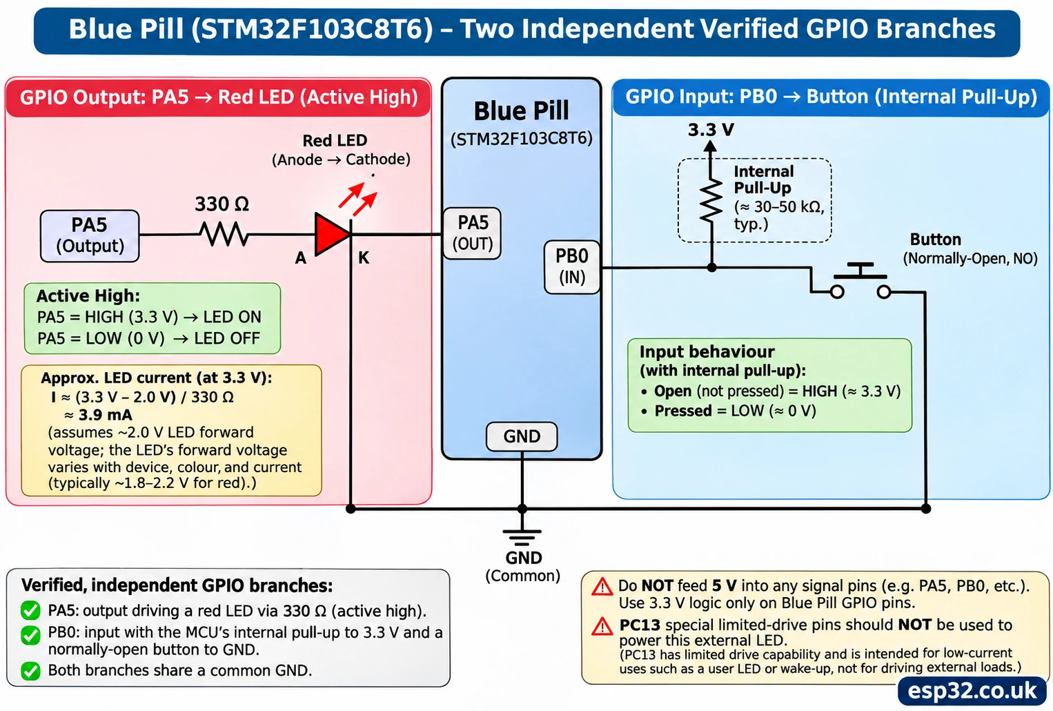
In CubeMX, mark PA5 as GPIO_Output, choose push-pull and low speed, and set its initial level low. Name the pin EXT_LED if desired. GPIOA’s peripheral clock must also be enabled by the generated initialization. Use this loop after regeneration:
/* External PA5 LED: high = ON, low = OFF. */
while (1)
{
    HAL_GPIO_WritePin(GPIOA, GPIO_PIN_5, GPIO_PIN_SET);
    HAL_Delay(250);
    HAL_GPIO_WritePin(GPIOA, GPIO_PIN_5, GPIO_PIN_RESET);
    HAL_Delay(750);
}
The external LED should now be on for a quarter second and off for three quarters of a second, once per second overall. If it does not work, inspect the resistor and LED orientation, continuity, ground reference and actual board pin identity. Do not connect an LED between PA5 and a 5 V supply or assume that an unpowered Blue Pill will tolerate an externally driven GPIO. Use 3.3 V logic for this tutorial.
Read a push button using a GPIO input and internal pull-up
A button demonstrates the reverse direction of GPIO: instead of driving an external component, the MCU reads an electrical state. Connect a normally-open push button from PB0 to GND. In CubeMX mark PB0 as GPIO_Input and enable Pull-up. Then open switch = logical high; pressed switch = logical low. The internal pull-up defines the inactive state without an extra external resistor, provided you do not attach other incompatible circuitry to PB0.
A minimal button-controlled indicator loop is:
while (1)
{
    GPIO_PinState pressed = HAL_GPIO_ReadPin(GPIOB, GPIO_PIN_0);
    HAL_GPIO_WritePin(GPIOA, GPIO_PIN_5,
                      pressed == GPIO_PIN_RESET ? GPIO_PIN_SET
                                                 : GPIO_PIN_RESET);
    HAL_Delay(10);
}
This assumes PB0 is an input pull-up and PA5 is a push-pull output. Pressing the button grounds PB0 and lights the external LED. This example simply mirrors the button state; it is not a debounced one-press/one-action interface. For a toggle-on-each-press project, you must recognise a stable transition and suppress the electrical chatter when the contacts close and open.
Debounce a button without freezing the whole application
Mechanical buttons can make and break contact several times in a few milliseconds. In small demos, a HAL_Delay(20) immediately after detecting a press may seem sufficient, but it blocks the CPU, can miss short events, and makes future tasks unresponsive. A more scalable pattern uses HAL_GetTick() and records when the raw button level last changed. After the state remains unchanged for, say, 25 ms, update the debounced state.
The following is an illustration of the key loop logic. Initialise lastRaw and stable from the input pin after MX_GPIO_Init() and set lastChange to HAL_GetTick() before entering the loop.
/* Define these variables before the while loop. */
GPIO_PinState lastRaw = HAL_GPIO_ReadPin(GPIOB, GPIO_PIN_0);
GPIO_PinState stable = lastRaw;
uint32_t lastChange = HAL_GetTick();

while (1)
{
    GPIO_PinState raw = HAL_GPIO_ReadPin(GPIOB, GPIO_PIN_0);
    uint32_t now = HAL_GetTick();

    if (raw != lastRaw) {
        lastRaw = raw;
        lastChange = now;
    }
    if ((uint32_t)(now - lastChange) >= 25U && stable != raw) {
        stable = raw;
    }

    HAL_GPIO_WritePin(GPIOA, GPIO_PIN_5,
                      stable == GPIO_PIN_RESET ? GPIO_PIN_SET
                                                : GPIO_PIN_RESET);
}
The subtraction on an unsigned 32-bit millisecond tick also behaves sensibly across the normal timer counter rollover for intervals shorter than half the counter range. This code is still a polling approach, but it avoids a blocking delay in every loop and provides a better foundation for small user interfaces. Later in the series, a dedicated STM32 interrupts article will explain EXTI callbacks and the NVIC.
GPIO output, button input and an interrupt are different things
The status LED needs an output. The direct button read needs an input. An external interrupt adds a hardware event mechanism so a configured edge can request CPU attention instead of requiring continuous polling. All three may use similar physical pins, but CubeMX produces different configuration values and, for interrupts, startup and IRQ code.
For a slow human button the polling technique above is usually sufficient. For an encoder, a fast pulse capture or a strict low-power wakeup requirement, carefully configured interrupts or timer input-capture peripherals are often a better fit. Do not put a long HAL_Delay() in a GPIO interrupt callback: callbacks should perform the smallest necessary work and defer non-urgent processing to the main execution context.
Likewise, toggling a pin in while (1) is not a substitute for hardware timer output when frequency, duty cycle and jitter matter. An STM32 timer running PWM can keep an output waveform alive while the processor does other tasks. A HAL_Delay() blink proves basic GPIO, flashing and clock operation; it is not a timing-performance benchmark.
Why is the LED blinking at the wrong speed?
HAL_Delay(500) is intended to wait roughly 500 milliseconds when the HAL tick source is correctly configured. The tick normally increments through a 1 ms timebase, commonly SysTick. If someone changes interrupt priorities, disables interrupts for long periods, changes the system clock without updating the HAL timebase or replaces the standard tick source incorrectly, the observed timing can be wrong or stop entirely.
Be especially careful with manually edited SystemClock_Config() code copied from an F4 or G4 tutorial. F103 clock-tree and PLL settings are different, and a board with a missing crystal will hang in HSE-ready checking if you configure it for an external source that never starts. Using the HSI default keeps a first LED lesson more reproducible. If you later select 72 MHz operation, the common 8 MHz HSE ×9 scheme is only appropriate when the particular board really has and supports that clock source.
A useful diagnostic is to put a breakpoint just after MX_GPIO_Init(), inspect the GPIO registers, and verify that code enters the infinite loop. If the debugger reaches Error_Handler() during the clock setup, fix the oscillator or PLL choice before changing LED wiring. If code runs but PC13 output does not change, inspect its mode and whether a later function reinitialises the same pin.
Troubleshooting: LED remains off, on or unpredictable
The quickest way to solve a first GPIO problem is to separate power, programming, pin configuration and external circuit. Trying a different GPIO before knowing that SWD works often makes the fault harder to isolate.
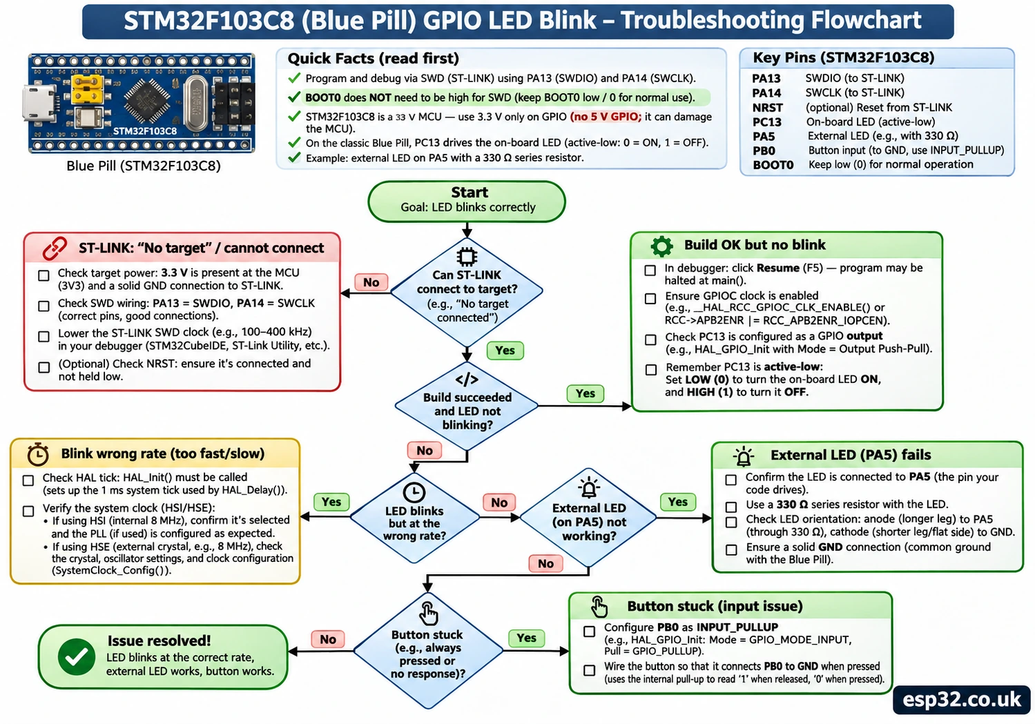
| Symptom | Likely cause | First useful check |
|---|---|---|
| ST-LINK recognised, target not found | No 3.3 V, swapped SWD lines, wrong probe selection, reset issue | Measure target 3.3 V; confirm PA13/PA14 and common GND |
| Firmware builds but LED never changes | Debugger halted, not actually flashed, wrong port/pin | Resume debugger; confirm flash verification and GPIOC PC13 |
| LED always on | PC13 held low, initial mode wrong, hardware defect | Inspect GPIO output and HAL writes; test GPIO_PIN_SET |
| LED always off | PC13 held high, wrong board LED pin, damaged LED | Test GPIO_PIN_RESET; check actual board schematic |
| Wrong blink rate | Faulty timebase or incorrect clock configuration | Start from CubeMX HSI defaults; inspect HAL_GetTick() |
| Code freezes before main loop | HSE/PLL startup failure or Error_Handler() | Inspect SystemClock_Config() and oscillator selection |
| External LED fails but PC13 works | LED polarity/resistor/PA5 wiring error | Check PA5 → resistor → LED → GND and GPIOA clock |
| Button input fluctuates | Floating PB0, incorrect pull-up or button wiring | Enable PB0 pull-up, connect switch to GND |
| USB cable connected, no programmer | Cable/USB device confusion | Connect PC to ST-LINK USB data port |
| Project stops working after regeneration | Custom code outside user-code blocks | Move changes into protected USER CODE regions |
The built-in LED is lit immediately but never blinks
An active-low LED might initially light during reset or before the configured output state takes effect. That brief behavior is not evidence that the application is executing. Verify that the output actually toggles after main() runs. If the LED remains lit, inspect whether the code writes GPIO_PIN_RESET continuously or never reaches the toggle. A simple debug breakpoint and live view of GPIOC output state are more informative than adding extra delays.
GPIOC cannot be found or the compiler complains about a pin symbol
Check that this is really an STM32F1 HAL project and that you included the generated main.h and stm32f1xx_hal.h transitively as intended by CubeMX. GPIOC and GPIO_PIN_13 are HAL/CMSIS symbols; a project generated for the wrong family or configured with a different library may not expose identical definitions. Avoid copying a project made for a NUCLEO-G431RB directly into an F103 build directory.
If you assigned the label LED_PC13 in CubeMX, it may generate macros such as LED_PC13_Pin and LED_PC13_GPIO_Port in main.h. Those generated names are convenient but depend on the exact label. Use the actual generated names instead of assuming all example projects call them LD2_Pin or USER_LED_Pin.
The button works only when touched or responds randomly
A floating digital input is neither reliably high nor low. Make sure PB0 has an enabled internal pull-up and the button makes a genuine connection to GND only while pressed. On a breadboard, buttons often bridge contacts on the same side internally; rotate or reposition the switch if you are accidentally shorting two permanently connected legs. Confirm the selected pin really is PB0 and has not been configured as analog or a different peripheral.
Flashing suddenly stopped after changing GPIO assignments
Do not use PA13/PA14 as ordinary outputs while relying on the same pins for SWD debugging. Leave the serial-wire debug configuration enabled in CubeMX. If bad application firmware prevents a normal attachment, connect under reset with ST-LINK and lower the SWD frequency. Before doing any erase or option-byte change, verify the target identity, supply and debug cable. This is a recoverable configuration problem in many cases, not automatically a damaged MCU.
GPIO coding mistakes that are easy to avoid
Using a physical connector number instead of a GPIO name. On the F103, PA5 and PC13 mean silicon port signals. A header drawing may show a different physical location on different boards. Always map the MCU signal to the board header using its board schematic.
Leaving the peripheral clock disabled. STM32 peripherals are clock-gated to reduce power consumption. CubeMX normally inserts __HAL_RCC_GPIOx_CLK_ENABLE(), but hand-written initialization must do so too. Writing a pin without first enabling the appropriate GPIO peripheral clock will not configure it as intended.
Copying an active-high example onto an active-low LED. Nucleo LD2 examples often set the pin high to light the LED. The standard Blue Pill PC13 indicator normally needs low. The same HAL_GPIO_TogglePin() API works for both because toggling reverses either level, but explicit ON/OFF logic must account for board wiring.
Forgetting that HAL delays block. A 500 ms delay is fine for a beginner LED. It becomes a problem when trying to handle a fast serial protocol, a precise PWM output, an encoder or multiple responsive tasks. The right progression is GPIO, then a tick-based scheduler or interrupts, then hardware timers and DMA where appropriate.
Assuming output speed is a desired blink frequency. GPIO_SPEED_FREQ_LOW configures output characteristics, not a 1 Hz timer. The blink rate comes from HAL_Delay() in this example. For a frequency-controlled waveform, use a timer rather than repeatedly changing GPIO in software.
Connecting directly to external loads. A GPIO is a logic interface, not a relay driver or motor power supply. Use an appropriate transistor or MOSFET driver, a flyback path for inductive loads, and verified current limits. Never connect an AC load to a GPIO. This basic LED tutorial intentionally uses only small currents through a series resistor.
Common questions about STM32 GPIO blinking
Does STM32CubeIDE 2.x still configure pins directly?
The normal CubeIDE 2.x workflow uses standalone STM32CubeMX for MCU pin, clock and peripheral configuration, then imports the generated project into CubeIDE. Existing older guides may show a combined application. The generated HAL code follows the same general initialization logic, but the tools are now separate.
Can I program the Blue Pill through its Micro-USB connector?
Not with a fresh stock STM32F103C8 expecting factory ROM USB DFU. You can upload with SWD/ST-LINK or the factory USART1 ROM loader, and user-installed USB bootloader firmware is a separate possibility. Merely raising BOOT0 on a typical F103C8 does not expose a native DFU USB drive.
Why does PC13 read high when the LED is off?
Because on common Blue Pill hardware the LED is tied toward the 3.3 V supply and PC13 sinks the current. High means no useful voltage difference through the LED; low turns the LED on. Check your specific board revision if it behaves differently.
Can I replace the 330 Ω resistor with no resistor?
No. An LED behaves nonlinearly, and directly connecting it to a GPIO can force excessive current. Select a resistor based on supply voltage, expected forward voltage, desired current and MCU pin limits. 330 Ω is a conservative demonstration choice for a small red indicator from an ordinary 3.3 V GPIO.
Why does the ST-LINK LED light while the Blue Pill LED remains dark?
Those LEDs belong to different devices. The programmer’s LED can indicate USB power even when the target STM32 is unpowered or its application has not started. Check the target rail and debug connection independently.
Is the same example valid on STM32F401 or STM32G431 boards?
The HAL API calls are conceptually similar, but the LED pin, electrical drive, peripheral initialization and RCC settings may differ. For example, a NUCLEO-F401RE’s LD2 uses PA5, and a NUCLEO-G431RB also has board-specific routing and clock choices. Regenerate the project for the exact MCU and check its board manual rather than copying the F103’s GPIO clock and PC13 setup.
How can I make two LEDs blink at different rates?
Use a millisecond tick or hardware timers instead of chaining blocking HAL_Delay() calls. Track separate deadline variables with HAL_GetTick() and toggle each configured output when its interval elapses. Timer interrupts are useful when the project grows and timing requirements justify them.
What to build after your first LED
A successful blink confirms that the toolchain, compiler, debugger, flash, runtime clock, GPIO configuration and one output path all work together. It does not test UART signal integrity, CAN transceivers, USB device enumeration, ADC reference accuracy or low-power current consumption. Treat it as the starting point for an engineering checklist, not a comprehensive board acceptance test.
The next step is typically to add a button, then sample a sensor over ADC or I²C, or use a hardware timer for PWM. Keep the STM32CubeMX .ioc in version control and make each change separately. You will learn more from three clean working experiments than from enabling six peripherals at once and then guessing which one caused a failure.
In this esp32.co.uk/ article, we have deliberately separated the MCU pin, the development-board LED circuit, the HAL API and the programmer wiring. That habit transfers directly to larger STM32 projects: confirm the electrical layer and the configuration before interpreting the firmware result. The Blue Pill’s PC13 LED is a convenient first indication, while an external PA5 LED and a PB0 button teach the general-purpose GPIO concepts you can reuse.
References and related esp32.co.uk/ guides
- ST — STM32F103x8/xB official datasheet, including the PC13–PC15 output restrictions and the 3.3 V electrical limits.
- ST — STM32CubeMX official product and code-generator description.
- ST — STM32F1 HAL GPIO driver.
- ST — STM32CubeF1 example for GPIO toggling.
- esp32.co.uk/ — Blue Pill Arduino IDE 2 installation and upload.
- esp32.co.uk/ — STM32CubeIDE and CubeMX setup.
- esp32.co.uk/ — STM32 GPIO voltage and 5 V tolerance.
Electrical diagrams and examples are documentation-based and have not been bench-tested on every Blue Pill revision. Confirm the exact board and power configuration before making connections.