
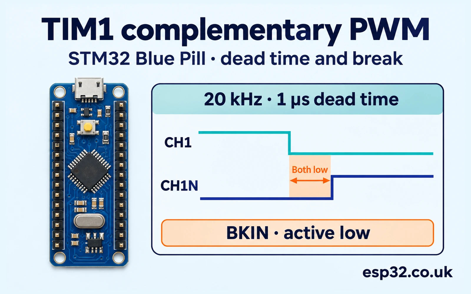
TIM1 on the STM32F103C8PriceAliExpress price can generate two related PWM outputs from one compare channel, insert a gap between their active intervals and gate both outputs through a hardware break input. In this esp32PriceAliExpress price.co.uk/ guide, you'll set up TIM1 on a Blue PillPriceAliExpress price, observe a 20 kHz complementary pair and verify that an active-low break stays gated until you explicitly arm it again.
Quick answer. Use PA8 for TIM1_CH1, PB13 for TIM1_CH1N and PB12 for TIM1_BKIN with the default pin mapping. At an 8 MHz TIM1 clock, set PSC to 0, ARR to 399 and CCR1 to 200. Use CKD DIV1 and dead-time code 8 for a nominal 1 µs gap. Enable break with low polarity, select low idle levels and leave automatic output disabled. Connect only a 3.3 V-compatible instrument and a break test jumper or switch for this logic-level lab.
Wire the logic-level test
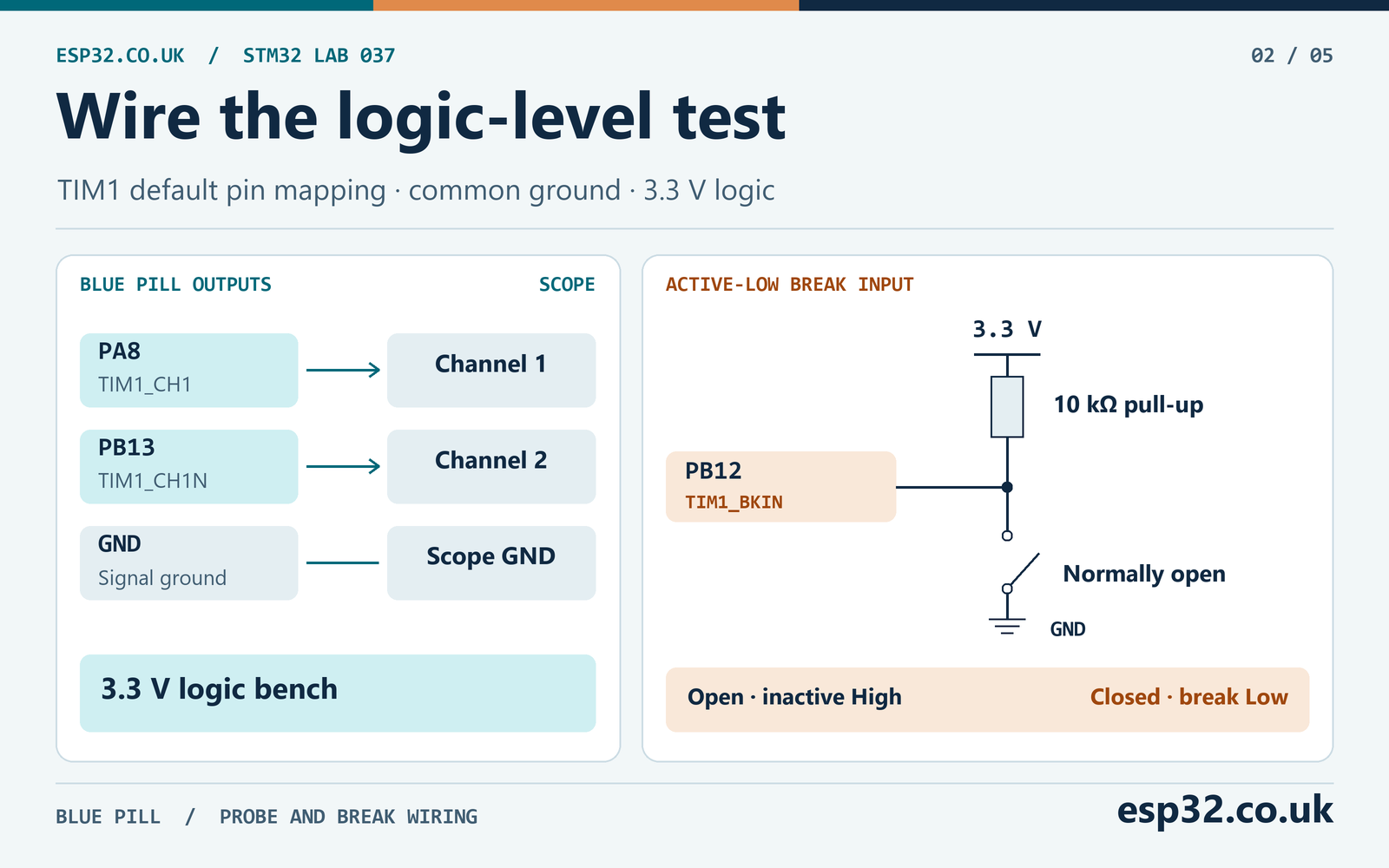
Use an STM32F103C8 Blue Pill, a working SWD probe and a two-channel oscilloscope or logic analyser suitable for 3.3 V logic. A third channel lets you capture the break signal with both outputs. Add a 10 kΩ resistor and a jumper or normally open momentary switch for the break input. The waveform checks in this lab are made at the MCU pins with no gate driver, motor or power switch connected.
| Blue Pill pin | TIM1 signal | Bench connection |
|---|---|---|
| PA8 | CH1 | Instrument channel 1 |
| PB13 | CH1N | Instrument channel 2 |
| PB12 | BKIN | 10 kΩ pull-up to 3.3 V and switch or jumper to ground |
| GND | Signal reference | Instrument ground and switch return |
Keep the TIM1 default pin mapping. Check the labels on the board before connecting the instrument. The PA8 pin is also available as a clock output on this MCU, and PB12 and PB13 can serve SPI2. CubeMX should give each pin one function in this project. Check both the alternate-function mapping and the GPIO modes in the generated code. STM32F103C8 Blue Pill pinout
Connect PB12 to 3.3 V through the resistor, then use the switch to connect PB12 to ground. With the switch open, the resistor makes the break input inactive. With the switch closed, PB12 is low and the resistor limits the current from the rail to about 3.3 V ÷ 10 kΩ = 0.33 mA. Use the jumper on PB12 only. PA8 and PB13 are push-pull outputs once the project has configured their GPIOs.
The pull-up defines the external break level during startup. A pull-up bench switch does not detect a broken wire, so treat it as a convenient test stimulus. Check PB12 at the MCU before attempting to arm. With an open switch, a low level points to wiring, a conflicting pin configuration or a faulty connection. With the switch closed, the pin should read low. Keep all probe grounds on the same board ground and use short probe leads when measuring a 1 µs gap. Blue Pill GPIO voltage and wiring guide
Configure TIM1 in STM32CubeMX
Create an STM32F103C8 C project and keep Serial Wire debugging enabled. Use HSI at 8 MHz with AHB and APB2 undivided for this lab. TIM1 is on APB2. With APB2 divided by one, its timer clock is the same as PCLK2. The STM32F1 timer clock relationship changes when the APB prescaler is greater than one. Read the actual TIM1 timer clock from the generated clock tree before calculating the timer values. CubeMX and STM32CubeIDE setup guide
Select TIM1’s internal clock and the PWM channel that exposes CH1 and CH1N. Check that both PA8 and PB13 are assigned to TIM1. Enable its break input on PB12. CubeMX versions can group the mode and break controls differently. Compare the generated HAL_TIM_PWM_Init(), HAL_TIM_PWM_ConfigChannel() and HAL_TIMEx_ConfigBreakDeadTime() calls with the settings below. The output pins use alternate-function push-pull. The break pin is an input on STM32F1 and the external resistor supplies its pull-up.
| Timing or channel parameter | Lab value | Result |
|---|---|---|
| TIM1 clock source | Internal, 8 MHz | Known clock for both calculations |
| Counter mode | Up, edge-aligned | One count cycle per PWM period |
| PSC | 0 | Counter clock remains at 8 MHz |
| ARR | 399 | Counts 0 through 399 |
| Repetition counter | 0 | Normal update every period |
| Clock division CKD | DIV1 | tDTS is one TIM1 clock period |
| Channel 1 mode | PWM mode 1 | Internal reference high while CNT is below CCR1 |
| CCR1 pulse | 200 | Reference duty is 200/400 |
| CH1 and CH1N polarities | High | Active pulses are high on both pins |
| Idle states OIS1 and OIS1N | Reset | Low idle levels for the pair |
| Break and dead-time parameter | Lab value | Why it matters |
|---|---|---|
| Dead-time code | 8 | Eight tDTS periods in the first encoding range |
| OSSR | Enabled | Select the timer’s run off-state handling |
| OSSI | Enabled | Keep timer control of the configured outputs with MOE clear |
| Lock level | Off | Preserve the ability to edit the bench configuration |
| Break state | Enabled | Allow the hardware break path |
| Break polarity | Low | Grounding PB12 asserts break |
| Automatic output AOE | Disabled | Require software to set MOE again |
| TIM1 break interrupt | Disabled for the lab | Let hardware gate the outputs and inspect the flag in foreground code |
Leave auto-reload preload disabled for the fixed period used here. HAL’s PWM channel configuration normally enables the compare preload. The lab sets its timing once and does not change the period or compare value while running. If you later change both values together, check how the preload and update event transfer them so you can avoid a mismatched period and compare value for one cycle. The STM32 timer, PWM and input capture guide covers the basic counting and update concepts.
TIM1 has several gates between the internal compare reference and the output pin. CEN enables counting. CC1E and CC1NE enable the main and complementary output paths. MOE is the main output enable for the advanced timer. The GPIO alternate function is the final connection to the pin. A changing CNT confirms the counter clock. It does not by itself confirm any of the output gates.
Calculate the PWM period and non-overlap
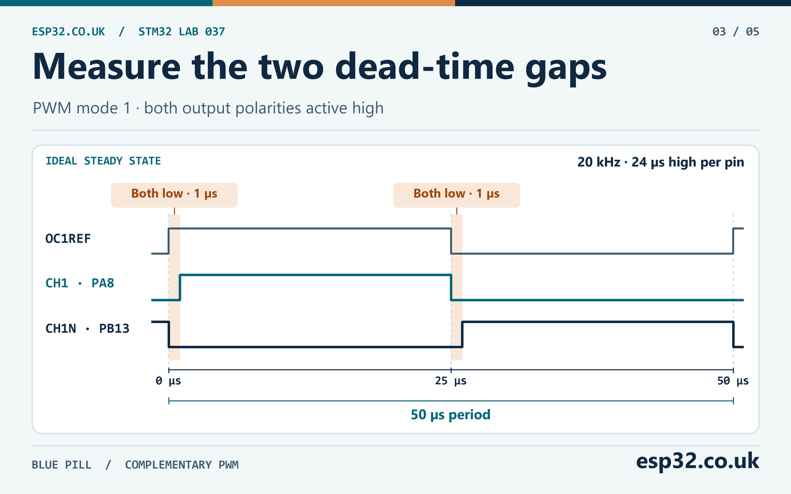
For this edge-aligned up-counter, the period includes ARR + 1 counts. At 8 MHz, with PSC equal to zero and ARR equal to 399, the frequency is 8,000,000 ÷ (1 × 400) = 20,000 Hz. Each period is 50 µs. In PWM mode 1 the reference is active for the first 200 counts of the period, giving a 25 µs reference interval and a 50% reference duty.
When both channel outputs are enabled and their polarities are active high, the dead-time generator delays the turn-on edge of each output. The currently active pin goes low, both pins stay low for the programmed gap, and then the other pin goes high. The resulting pin waveforms are complementary with two low-low intervals per period. An ideal inversion of the main pin would have no such gap.
For the lab, tDTS = 1 ÷ 8 MHz = 125 ns. Dead-time code 8 in the first range therefore gives 8 × 125 ns = 1 µs. In a steady-state cycle where the reference rises at time zero, the active-high CH1 pulse begins at 1 µs and ends at 25 µs. CH1N rises at 26 µs and goes low at the next reference rise at 50 µs. That gives 24 µs high on each output, or 48% duty per pin, although the reference is still set to 50%.
| Time within the ideal cycle | CH1 on PA8 | CH1N on PB13 |
|---|---|---|
| 0 to 1 µs | Low | Low |
| 1 to 25 µs | High | Low |
| 25 to 26 µs | Low | Low |
| 26 to 50 µs | Low | High |
Use the interval from one rising edge to the next rising edge on the same output to measure frequency. Use the time from the falling edge of one output to the rising edge of the other to measure the gap. These are different measurements. Check the non-overlap at both transitions. The expected numbers are calculated from the nominal oscillator and timer settings. A real trace also includes oscillator tolerance, pin transition times, probe loading and the instrument’s time resolution.
Predict when a pulse becomes too short
Changing the reference duty moves the changeover at CCR1 while the period remains set by ARR. With the same 50 µs period and a 10% reference duty, the reference would be high for 5 µs and low for 45 µs. Subtract the 1 µs turn-on delay from each interval to get 4 µs high on CH1 and 44 µs high on CH1N. That corresponds to 8% and 88% at the pins. These values assume the compare setting stays within the normal PWM range and the two active intervals are longer than the delay.
At this timer rate, CCR1 equal to 5 would request a high reference interval of 0.625 µs. The 1 µs turn-on delay exceeds that interval, so the main pulse is suppressed. The reverse situation can happen near the other end of the duty range, when the reference is low too briefly for the complementary pulse. Use this calculation when a trace shows a missing pulse at an extreme duty.
For this example, both requested intervals have to exceed eight counter ticks because PSC and CKD are both undivided. That gives CCR1 values from 9 through 391 for nonzero ideal high intervals on both outputs. Those endpoints leave only one tick of high time on one output. The usable range for an actual load would depend on its minimum pulse width and the measurement margin. The supplied firmware keeps its fixed 50% reference.
Decode TIM1 dead-time values
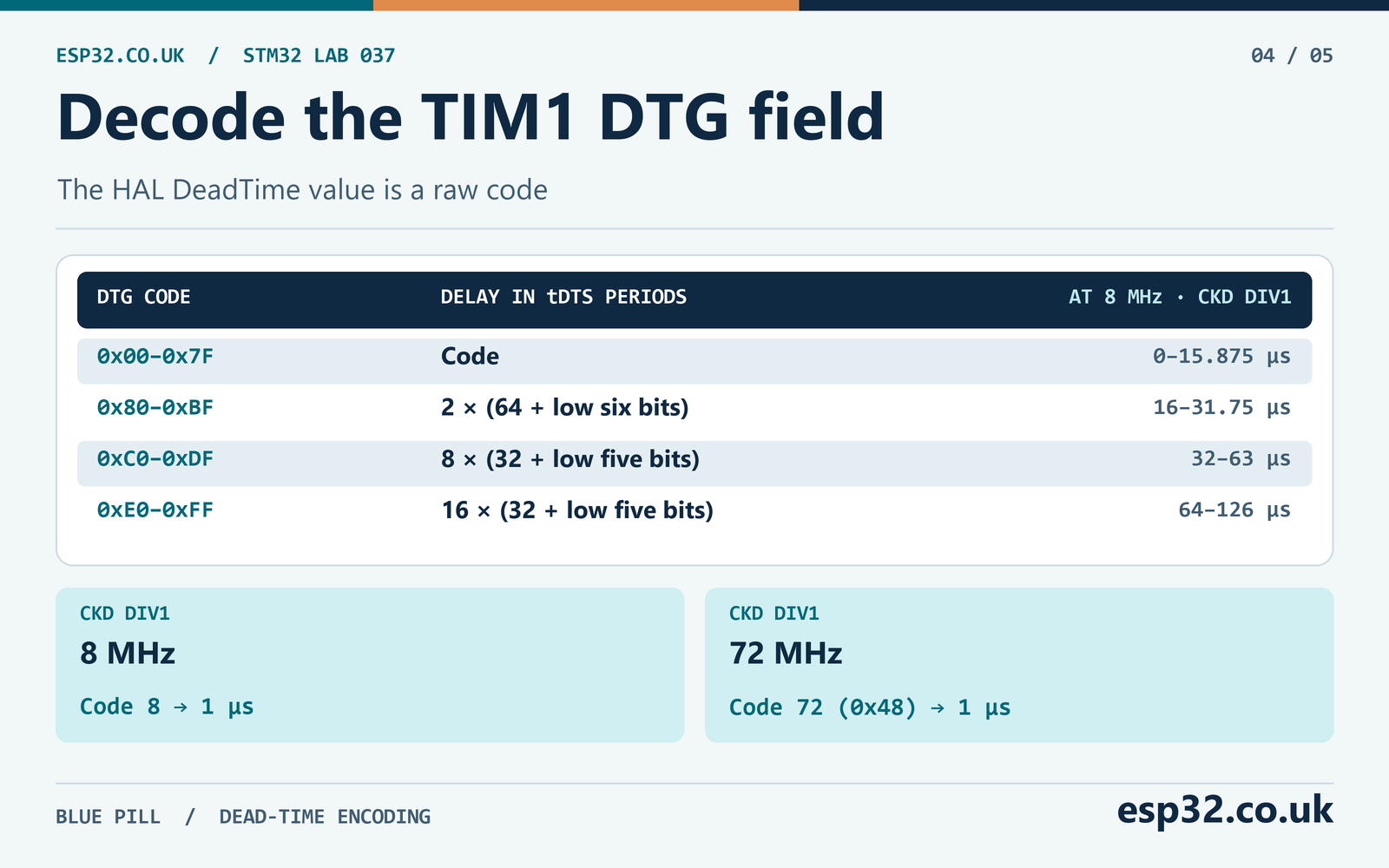
CubeMX and HAL_TIMEx_ConfigBreakDeadTime() take a raw DTG code. The code is an eight-bit field with four ranges. The low range increments by one tDTS. The higher ranges use a base count plus a low-bit field with a larger multiplier. Converting a desired time by dividing by tDTS only works directly in the first range.
| DTG code | Delay in tDTS periods | Time range at 8 MHz and CKD DIV1 |
|---|---|---|
| 0x00 to 0x7F | Code | 0 to 15.875 µs |
| 0x80 to 0xBF | 2 × (64 + low six bits) | 16 to 31.75 µs |
| 0xC0 to 0xDF | 8 × (32 + low five bits) | 32 to 63 µs |
| 0xE0 to 0xFF | 16 × (32 + low five bits) | 64 to 126 µs |
For an example outside the first range, a 20 µs delay at 8 MHz corresponds to 160 tDTS periods. In the second range, divide 160 by two and subtract 64. The low six-bit value is 16, giving code 0x90. This example illustrates the encoding. In a 20 kHz, 50% reference cycle, a 20 µs gap would leave only 5 µs of high time per pin. A gap at or above the requested active interval can suppress that pulse.
If you use a 72 MHz TIM1 clock with CKD still set to DIV1, the same code 8 represents only about 111 ns. A nominal 1 µs delay in the first range takes code 72, or 0x48. Keeping the 20 kHz frequency and 50% reference duty at that clock requires ARR 3599 and CCR1 1800 with PSC still zero. The shipped lab checks the original 8 MHz example’s timer register settings. To change the example, adjust the clock, timer parameters and lab checks together.
CKD changes the timing base for dead time and certain input sampling functions. The PWM count rate follows the timer clock and PSC. Changing PSC alone can change the PWM period without changing tDTS. Changing the timer clock can affect both. When you revise the settings, recompute frequency and delay separately and confirm them on the same trace.
Prepare both outputs before arming
Keep the generated HAL initialisation for the timer, channel and break/dead-time configuration. Add tim1_pwm_lab.h and tim1_pwm_lab.c to the project and build as C11. The lab owns TIM1 once prepared. Its preparation checks the fixed register configuration, enables both channel paths while the main output gate is closed and starts the counter. The timer can then run with the output pair in the configured idle state.
The standard HAL PWM and PWMN start calls each perform output-enable steps, including setting MOE for an advanced timer. Calling those start functions in sequence can open the main gate before both paths have been set up. The lab uses the generated HAL setup and a short register-level sequence for the start and stop actions, so it can hold MOE low during preparation. Keep those actions in one foreground owner. Use the lab’s arm and disarm functions for this timer after preparation.
#ifndef STM32_037_TIM1_PWM_LAB_H
#define STM32_037_TIM1_PWM_LAB_H

#include "stm32f1xx_hal.h"
#include <stdbool.h>
#include <stdint.h>

enum {
    PWM_LAB_PREPARED = 1U << 0,
    PWM_LAB_OUTPUTS_ENABLED = 1U << 1,
    PWM_LAB_BREAK_ACTIVE = 1U << 2,
    PWM_LAB_BREAK_FLAG = 1U << 3
};

bool PwmLab_Prepare(TIM_HandleTypeDef *timer);
bool PwmLab_Arm(void);
void PwmLab_Disarm(void);
uint32_t PwmLab_Status(void);

#endif
#include "tim1_pwm_lab.h"
#include <stddef.h>
static TIM_HandleTypeDef *owned_timer;
static bool break_active(void)
{
return HAL_GPIO_ReadPin(GPIOB, GPIO_PIN_12) == GPIO_PIN_RESET;
}
static bool break_flag(void)
{
return __HAL_TIM_GET_FLAG(owned_timer, TIM_FLAG_BREAK) != RESET;
}
bool PwmLab_Prepare(TIM_HandleTypeDef *timer)
{
if (owned_timer != NULL || timer == NULL || timer->Instance != TIM1) {
return false;
}
TIM_TypeDef *tim = timer->Instance;
const uint32_t bdtr_mask = TIM_BDTR_DTG | TIM_BDTR_LOCK | TIM_BDTR_OSSI |
TIM_BDTR_OSSR | TIM_BDTR_BKE | TIM_BDTR_BKP |
TIM_BDTR_AOE | TIM_BDTR_MOE;
const uint32_t bdtr_expected = TIM_BDTR_OSSI | TIM_BDTR_OSSR | TIM_BDTR_BKE | 8U;
const uint32_t pwm1 = TIM_CCMR1_OC1M_2 | TIM_CCMR1_OC1M_1;
if (tim->PSC != 0U || tim->ARR != 399U || tim->CCR1 != 200U ||
(tim->CR1 & (TIM_CR1_CEN | TIM_CR1_DIR | TIM_CR1_CMS | TIM_CR1_CKD)) != 0U ||
(tim->SMCR & TIM_SMCR_SMS) != 0U ||
(tim->CR2 & (TIM_CR2_OIS1 | TIM_CR2_OIS1N)) != 0U ||
tim->CCER != 0U ||
(tim->CCMR1 & (TIM_CCMR1_CC1S | TIM_CCMR1_OC1M)) != pwm1 ||
(tim->BDTR & bdtr_mask) != bdtr_expected) {
return false;
}
/* Configure both channel enables while the main output gate is closed. */
SET_BIT(tim->CCER, TIM_CCER_CC1E | TIM_CCER_CC1NE);
SET_BIT(tim->CR1, TIM_CR1_CEN);
owned_timer = timer;
return true;
}
bool PwmLab_Arm(void)
{
if (owned_timer == NULL || break_active() ||
(owned_timer->Instance->BDTR & TIM_BDTR_MOE) != 0U) {
return false;
}
__HAL_TIM_CLEAR_FLAG(owned_timer, TIM_FLAG_BREAK);
if (break_active() || break_flag()) {
return false;
}
SET_BIT(owned_timer->Instance->BDTR, TIM_BDTR_MOE);
if (break_active() || break_flag() ||
(owned_timer->Instance->BDTR & TIM_BDTR_MOE) == 0U) {
PwmLab_Disarm();
return false;
}
return true;
}
void PwmLab_Disarm(void)
{
if (owned_timer != NULL) {
CLEAR_BIT(owned_timer->Instance->BDTR, TIM_BDTR_MOE);
}
}
uint32_t PwmLab_Status(void)
{
if (owned_timer == NULL) {
return 0;
}
uint32_t status = PWM_LAB_PREPARED;
if ((owned_timer->Instance->BDTR & TIM_BDTR_MOE) != 0U) {
status |= PWM_LAB_OUTPUTS_ENABLED;
}
if (break_active()) {
status |= PWM_LAB_BREAK_ACTIVE;
}
if (break_flag()) {
status |= PWM_LAB_BREAK_FLAG;
}
return status;
}The configuration checks the timer instance and key timing, mode, polarity, idle and break register settings. Verify the clock tree and GPIO setup separately. The function expects a fresh timer that hasn’t been started. If the prepare call fails, inspect the first mismatching register against the setup table. A failed prepare call leaves the timer under its previous owner.
Compare the register values before and after prepare
Halt immediately before the prepare call while the outputs are still gated. Read the timer registers after the HAL initialisers have finished. This lets you distinguish a mismatch in the generated timer setup from a failed attempt to arm. Inspect the mask and fields rather than comparing an unrelated bit in the same register.
| Register or field | Before prepare | After a successful prepare |
|---|---|---|
| PSC, ARR, CCR1 | 0, 399, 200 | Same programmed timing |
| CR1.CEN | 0 | 1 |
| CR1.CMS, DIR and CKD | Edge-aligned, up-counting, DIV1 | Same modes |
| SMCR.SMS | 0 for the lab’s internal clock mode | Same mode |
| CCMR1.CC1S and OC1M | Output and PWM mode 1 | Same channel mode |
| CCER | 0 | CC1E and CC1NE set, polarity bits clear |
| CR2.OIS1 and OIS1N | 0 and 0 | Low idle levels |
| BDTR configuration fields | 0x1C08 for the lab’s options | Same options and MOE still clear |
The value 0x1C08 combines break enable, run and idle off-state selection and DTG equal to 8. A successful arm adds the MOE bit, giving 0x9C08 in the implemented configuration fields. The break flag lives in SR, so it won’t appear in that BDTR value. When you read these registers after a break, expect the stored setup bits to remain available while MOE is low.
Read the timer as part of a whole peripheral. MOE applies across TIM1, so it is a poor fit for independently arming unrelated outputs on the same timer. The dedicated bench project uses only channel 1 and its complementary output. If the timer is shared in another project, account for every channel affected by a gate change.
Add the debugger commands
Put the include and variables in the generated user sections. Call PwmLab_Prepare() after MX_TIM1_Init() and the GPIO configuration. Place the request handling in the existing foreground loop. If both requests are pending when the disarm branch runs, it clears the pending arm before proceeding. The requests are a bench control, with one foreground reader.
/* USER CODE Includes */
#include "tim1_pwm_lab.h"

/* USER CODE PV */
volatile uint32_t pwm_arm_request;
volatile uint32_t pwm_disarm_request;
volatile uint32_t pwm_status;
volatile bool pwm_last_arm_ok;

/* USER CODE 2, after MX_TIM1_Init() and the GPIO setup */
if (!PwmLab_Prepare(&htim1)) {
    Error_Handler();
}

/* USER CODE 3, inside the generated while (1) loop */
if (pwm_disarm_request != 0U) {
    pwm_disarm_request = 0U;
    pwm_arm_request = 0U;
    PwmLab_Disarm();
}
if (pwm_arm_request != 0U) {
    pwm_arm_request = 0U;
    pwm_last_arm_ok = PwmLab_Arm();
}
pwm_status = PwmLab_Status();
The request executes when the foreground loop runs. Set a value in the debugger and resume the board. Read pwm_last_arm_ok as the result of the last arm attempt. Read pwm_status for the current observed state. The status fields come from separate register and pin reads, so a break that arrives during a read can change the next snapshot. Use the scope for the order and timing of the actual edges.
Check break and manual re-arm
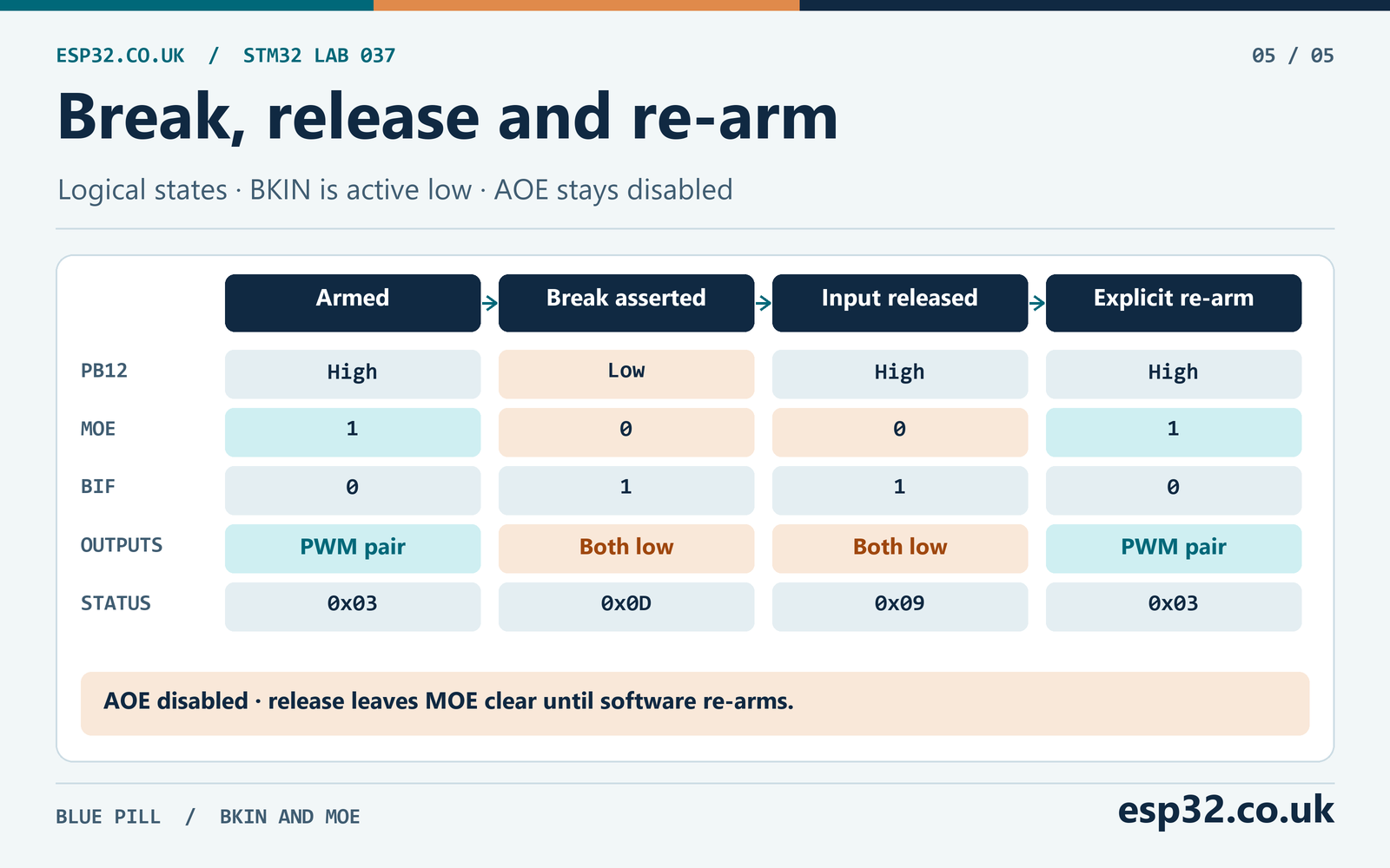
With break enabled and low polarity, grounding PB12 causes TIM1’s hardware break path to clear MOE. The hardware can do that without a timer interrupt handler or a foreground GPIO read. The break flag BIF records the event. With the two outputs configured as active high and both idle settings low, the pair should settle low while gated. The counter can keep running because gating the outputs is separate from stopping CEN.
When you release PB12, the pin returns high. Because AOE is disabled, this release leaves MOE cleared. Software must make a separate arm request. The lab checks the inactive input, clears the previous break flag, checks for a break again and then tries to set MOE. It checks the result and gates off if it observes a break during the attempt. This sequence is a bench acknowledgement policy. A pin read and a register write are separate operations, and a very brief input change can occur between them. The module should be used for the logic-only procedure shown here.
| Stable condition in the bench sequence | PB12 | MOE | BIF | Status |
|---|---|---|---|---|
| Prepared, no break history | High | 0 | 0 | 0x01 |
| Explicit arm accepted | High | 1 | 0 | 0x03 |
| Break held active | Low | 0 | 1 | 0x0D |
| Break released, before re-arm | High | 0 | 1 | 0x09 |
| Explicit re-arm accepted | High | 1 | 0 | 0x03 |
| Software disarm after a clean arm | High | 0 | 0 | 0x01 |
The pin level describes the present external stimulus. The flag can remain set after that stimulus is gone. An application that needs to record the cause should save its diagnostic data before acknowledging the flag. The STM32F1 also has internal break-related paths, so PB12 alone does not identify the cause of every break event. This HSI bench setup tests the external pin.
ST’s ES096 errata describes a system-break case where PWM can resume on a following cycle in automatic output mode. The lab leaves AOE cleared and uses explicit acknowledgement. Treat the F103 reference manual and device errata as the authorities for this target when reading a newer STM32 break example. Other families can add controls such as input filters and multiple break inputs that this TIM1 configuration doesn’t expose.
Measure the two outputs on the bench
Flash the project using SWD. Start with PB12 high and run the application after reset. Check that preparation succeeded and that PA8 and PB13 are low once the timer owns the pins. The first status should be 0x01 if there has been no break. Verify that the prepared state has CEN set and MOE clear. If a probe shows activity before the first arm request, inspect the pin mapping, generated start calls and MOE. STM32CubeProgrammer and SWD flashing guide
Set pwm_arm_request to 1 and resume. Inspect a steady section of waveform after the arm. An explicit MOE write can happen at an arbitrary counter phase, so use complete cycles after the first output transition for the frequency and dead-time measurements. Trigger on PA8 rising and check the next PA8 rising edge about 50 µs later. Measure the high time on PA8 and PB13. Then zoom into each changeover and measure from the falling edge on the outgoing pin to the rising edge on the incoming pin.
If your logic analyser samples at 20 MS/s, adjacent samples are 50 ns apart, giving roughly 20 sample intervals across 1 µs. That is sufficient to make the intended gap visible on a clean logic trace. The timing quantisation and input threshold still affect the reported width. Use an oscilloscope if you need to see signal shape, rise and fall times, or the effect of probe loading. Compare both signals with consistent trigger and threshold settings.
With the PWM running, ground PB12 through the switch or jumper connection. If a third channel is available, trigger on PB12 falling and capture both output pins. The active pin should stop switching and both pins should settle low. There may be switch bounce. Keep the input held long enough to verify a stable low state and check BIF and MOE after the capture. If using two instrument channels, first capture the PWM pair, then repeat with PB12 and one PWM pin to see their timing relationship.
Release PB12 and leave the firmware running. Several complete PWM periods should pass with both outputs still low. An explicit arm request should bring the pair back. Repeat once while holding PB12 low before requesting arm. The request should fail and the pins should stay low. Then release, arm, and test pwm_disarm_request. The software disarm should close MOE while the counter and channel enables remain set.
| Bench check | Expected observation |
|---|---|
| First run after reset | Both pins idle after preparation |
| Steady state after arm | About 20 kHz, 24 µs high on each pin |
| Each output changeover | About 1 µs with both pins low |
| PB12 grounded while armed | MOE cleared, BIF set, pins settle low |
| PB12 released | BIF retained and no PWM until the next arm request |
| Arm attempted with PB12 still low | Rejected |
| Software disarm | Pins gated low while CEN stays set |
The lab compiled and linked for Cortex-M3 with ST’s startup, TIM and TIMEx drivers. Native tests ran the same gating code with mocked registers and PB12 reads. Those tests checked the software paths and injected a break during re-arm. Check the real pin voltage, break response and timing with the procedure above.
Test power-up with the break held
Use a separate run for the startup case. Hold PB12 low before releasing reset and leave it low while the firmware configures GPIO and TIM1. Observe the pins after preparation. A pending break can produce 0x0D once the timer and break source have been configured. A deliberate arm request during this held condition should leave both pins low. Release the switch and check that the gate remains closed even though the external signal is now inactive.
Check the same sequence after a normal power cycle and a debugger reset. A reset restarts the software variables and the register setup. The arm request is a RAM variable that starts at zero. Check that your debugger’s startup commands don’t write it automatically. If a breakpoint holds the CPU during the test, remember that debug freeze options can affect whether TIM1 keeps counting. Use continuous execution for the waveform test.
For a repeatable record, capture the external input and both outputs, and note the clock and DTG code alongside the trace. Include a clean armed period, the first asserted break and a stable gated interval after release. Capture the later re-arm separately if the instrument’s memory is too short to show both in detail. That separates the time to gate the active pin from the operator’s time to acknowledge the event.
Read the off-state configuration from the pins
MOE low is an internal gate condition. The resulting level at a pin depends on the channel enables, polarity, idle state and off-state configuration. With both enables configured, OSSI enabled and the idle levels set low, the timer is intended to drive the configured outputs low in the gated state. With a different OSSI setting the timer may release control of the output. Before GPIO initialisation, the pin is also in its reset configuration. These are separate states, so observe startup, armed operation and the gated state independently.
If you’re checking the instrument’s logic levels, measure the DC idle state after the firmware has run its GPIO and timer setup. A floating pin can appear low on a logic analyser because of the instrument input or board leakage. An oscilloscope shows the actual voltage. Compare the settings with the STM32F103 complementary output control table before changing polarity or idle-state values.
Check the instrument before interpreting a small gap
At the 8 MHz setup, one timer clock is 125 ns. A capture at 1 MS/s has one sample per microsecond, so a 1 µs interval is too close to its sampling step for a meaningful width measurement. Increase the capture rate and zoom around one changeover. Use the same thresholds for both channels. If the traces still show a difference between the two gaps, connect both instrument inputs to the same logic output in a separate test and check whether their reported edges line up. Keep both probe grounds on the board ground.
Use a stable section of the waveform for timing comparisons. A break can cut short the currently active interval, and the first active interval after re-arm can start at a different counter phase. These events are useful for checking the gate but can obscure the steady 24 µs high interval. Record the period, both high widths and both non-overlap gaps from steady cycles. A clock change scales the period and the dead time when their register settings stay fixed, while a DTG-only change should leave the period unchanged.
Troubleshoot TIM1 complementary PWM
| Symptom | First check | Likely area |
|---|---|---|
| CNT changes but both pins stay low | MOE, BKIN and BIF | Main output gate or active break |
| Only PA8 switches | PB13 pin mode and CC1NE | Complementary channel routing or enable |
| Outputs look like exact inverses | DTG, CKD and instrument resolution | Dead time absent or too short to resolve |
| A pulse disappears at one extreme of duty | Compare active interval with dead time | Requested pulse is too narrow |
| Measured period differs from 50 µs | TIM1 kernel clock, PSC and ARR | Clock tree or timer configuration |
| Outputs restart as soon as break clears | AOE and any repeated start calls | Automatic or software re-arm |
| Arm fails while PB12 reads high | MOE, BIF and timer ownership | Gate already open, break flag persists or prepare failed |
| Break flag appears intermittently | PB12 trace and ground reference | Input noise, bounce or conflicting pin use |
When a pin is quiet, follow the timer signal path. Verify CNT advances, then compare CCMR1, CCER and BDTR with the setup. If the count and compare are correct, confirm the GPIO alternate function and remap. For BKIN, measure the actual PB12 voltage at the board. Software printing the pin state helps after the fact, but a short break pulse can disappear before a UART message is sent. STM32 UART and HAL diagnostics guide
If the two measured gaps disagree, verify which pair of edges you’re measuring. The steady-state gap starts when one pin falls and ends when the other pin rises. Rise-to-rise across two different channels is closer to half a period in this example. Use the same scope voltage threshold on both channels, and exclude initial cycles after an arm or break.
Questions about STM32 complementary PWM
Why is each output 48% high when CCR1 requests 50%?
The compare makes the internal reference high for 25 µs in a 50 µs cycle. With active-high paired outputs, each turn-on edge waits 1 µs. Each pin then has 24 µs high, and the two 1 µs low-low gaps account for the remaining four percent of the period.
Is CH1N a second independent PWM channel?
CH1N is the complementary path associated with CH1. Both paths come from the same channel reference and use the same compare value in this configuration. Separate compare channels have their own references, while the DTG field and main output gate are shared at TIM1 level.
Does enabling the break interrupt make shutdown happen faster?
The hardware break path clears MOE. Enabling the interrupt adds software notification, which can log the event or coordinate recovery. The bench test leaves it disabled and reads BIF in the foreground.
Can I use the same dead-time code after changing the clock?
Recalculate tDTS from the clock and CKD, then use the right DTG range. At 72 MHz with CKD DIV1, code 8 gives about 111 ns while code 72 gives 1 µs. Recalculate the PWM period separately.
Datasheets & External Resources
| Source | What to check |
|---|---|
| ST DS5319 STM32F103x8/xB datasheet | Default PA8, PB13 and PB12 alternate functions |
| ST RM0008 reference manual | Complementary output timing, break behaviour, off-state table and DTG encoding |
| ST AN4013 timer overview | Advanced timer functions and complementary signals |
| ST AN4277 PWM shutdown application note | Break sources and PWM shutdown behaviour by MCU family |
| ST ES096 medium-density device errata | System-break re-enable limitation in automatic output mode |
| ST STM32F1 HAL TIM v1.1.10 and TIMEx v1.1.10 | PWM configuration, start behaviour and break/dead-time setup |