Quick answer: To connect a 3.3 V I²C sensor to an STM32F103C8PriceAliExpress price Blue PillPriceAliExpress price, connect PB6 to SCL, PB7 to SDA, and GND to GND. Power the sensor from a supply appropriate to its actual breakout, normally 3.3 V for an unregulated module. Fit or verify pull-up resistors from both SCL and SDA to 3.3 V (typically 4.7 kΩ for a short 100 kHz prototype). In STM32CubeMX, enable I2C1 as a master at 100000 Hz; in HAL, pass the device’s 7-bit address shifted one bit left, such as 0x76 << 1 for a BME280PriceAliExpress price whose SDO address-select pin is low. Do not attach RS-232, 5 V pull-ups or arbitrary LCD-backpack power rails to these pins.
In this tutorial, we go well beyond the customary four-wire diagram. We explain how I²C actually works, how to scan for addresses without confusing a 7-bit address with an 8-bit bus byte, how to read a BME280 chip ID and configure a sensor register, how to share the bus with an OLED, how to choose pull-ups and speeds, and how to diagnose SDA stuck low, NACK responses and the well-documented STM32F1 I²C peripheral limitations. The examples target the STM32F103C8T6, its classic STM32F1 HAL and ordinary Blue Pill development boards. Other STM32 families may have different I²C registers and CubeMX settings.
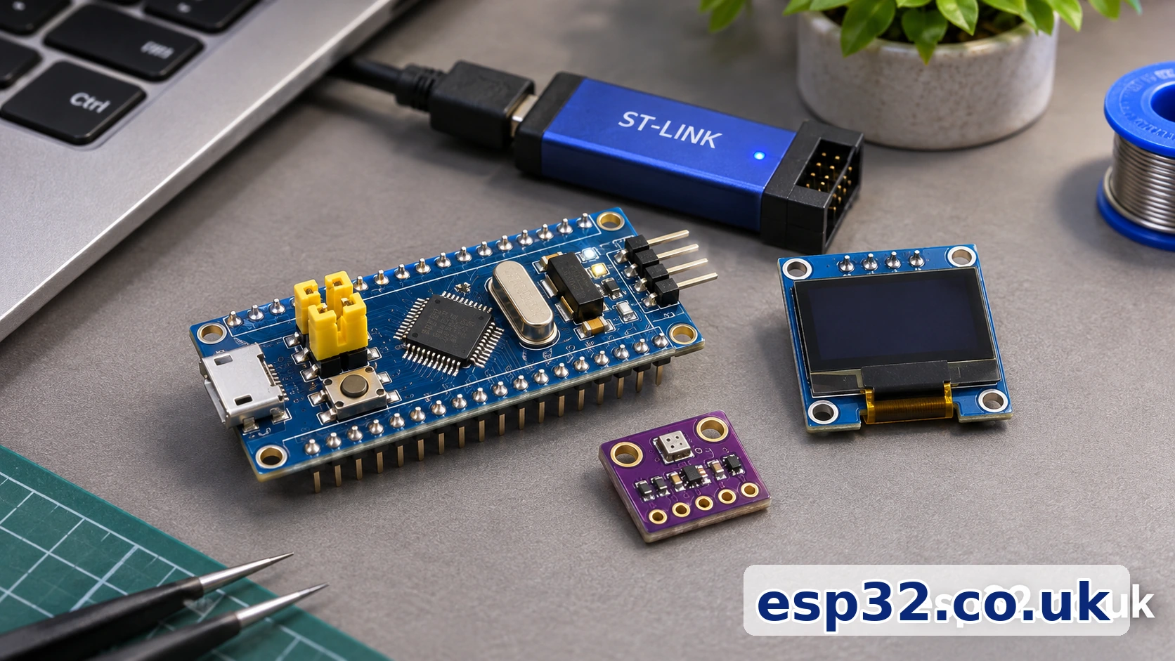
STM32F103 I2C pins and capabilities
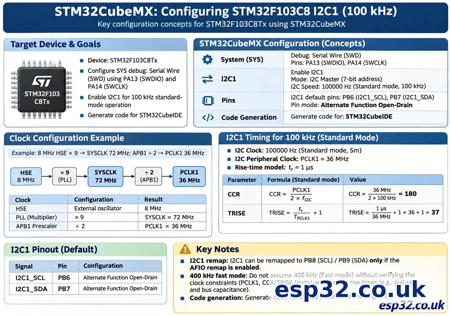
The STM32F103C8 has two I²C peripheral controllers, I2C1 and I2C2. On a common Blue Pill, the easiest starting point is I2C1 on PB6/PB7. The optional I2C1 remap moves those signals to PB8/PB9: it does not create another I²C controller. I2C2 uses PB10/PB11 on this family. Check any existing pin use, especially if your project has reassigned PB6/PB7 to a different peripheral.
| Interface | SCL | SDA | Notes |
|---|---|---|---|
| I2C1 default | PB6 | PB7 | Recommended for the first example; AF open-drain configuration |
| I2C1 remapped | PB8 | PB9 | Enable I2C1 remap in AFIO/CubeMX, not merely the pin labels |
| I2C2 | PB10 | PB11 | Separate controller; corresponding HAL handle is normally hi2c2 |
| ST-LINK SWD | PA14 SWCLK | PA13 SWDIO | Different interface; preserve these pins for debugging |
| USART1 default | PA9 TX | PA10 RX | Useful for diagnostic logs, but not part of the I²C bus |
The pin mappings are given in ST’s RM0008 reference manual. All the listed I²C pins are logical MCU signal names, not a promise about physical header positions on every third-party board. Check the printed pin labels and a trusted board schematic before attaching anything.
I²C supports multiple addressed devices on two shared signal wires. The F103 implementation supports standard-mode 100 kHz and fast-mode operation up to 400 kHz subject to electrical conditions, peripheral clocks and the exact silicon limitations. An I²C sensor’s advertised 400 kHz capability alone does not guarantee that long breadboard wires, four sets of pull-ups or an inappropriate APB1 clock will operate reliably at that rate.
What SCL, SDA and the pull-up resistors actually do
An I²C bus is not driven like a conventional push-pull UART output. The clock line SCL and data line SDA are typically driven low by participating devices and released to a high state through resistors. This is why the common configuration is alternate-function open-drain for the STM32 pins. An external pull-up to the allowed bus voltage provides a logical high when no one is pulling the line low.
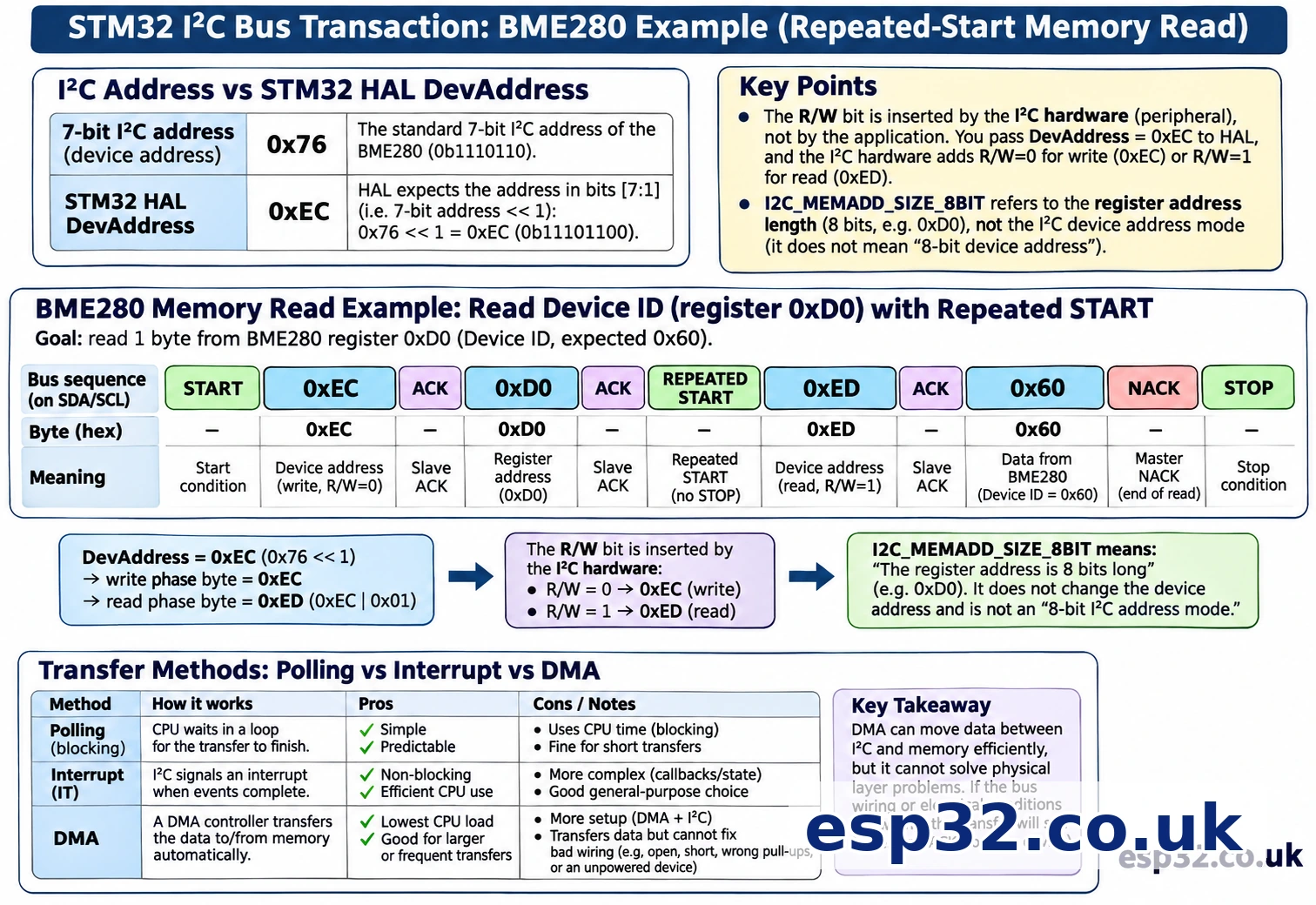
A controller initiates a transaction with a START condition, transmits an address and read/write bit, waits for an ACK from the addressed device, transfers one or more bytes, and ends with a STOP condition. The controller generally generates SCL, although a device may use clock stretching to hold it low temporarily. A repeated START lets a controller change transfer direction without releasing the bus, often when reading a register after sending its address.
| Term | What it means | Typical pitfall |
|---|---|---|
| SCL | Shared I²C clock | Confusing it with an SPI clock or leaving it without a pull-up |
| SDA | Bidirectional serial data | Swapping it with SCL or connecting it to a 5 V pull-up |
| START / STOP | Bus state transitions while SCL is high | Glitches or malformed framing lead to recovery difficulties |
| ACK / NACK | Receiver acknowledges or rejects a byte | A missing sensor usually returns NACK rather than an all-zero register |
| 7-bit address | Logical identity, e.g. 0x76 | Passing 0x76 unshifted to STM32F1 HAL’s DevAddress argument |
| Clock stretching | A device holds SCL low to delay transfer | A controller or timeout that cannot handle the device’s latency |
| Pull-ups | Resistive path to the allowed bus voltage | Missing, excessive or 5 V pull-ups cause unreliable or unsafe signals |
With a 4.7 kΩ resistor to 3.3 V on each line, the approximate static current in a line held low is (3.3 V - 0 V) / 4700 Ω ≈ 0.70 mA. This is normally modest. If several breakout boards each contain a pull-up, their resistances combine in parallel, which increases the current the active device must sink. Conversely, very weak pull-ups and long cables create slow rising edges that can break fast transactions.
The STM32F1 electrical implementation is not equivalent to a perfect idealised open-drain transistor in every power state. Do not treat a nominally five-volt-tolerant pin as permission to connect a 5 V I²C module or back-power a disconnected Blue Pill. Keep this first project on a single 3.3 V bus, with all grounds common.
Safe Blue Pill wiring for a 3.3 V sensor
For the first experiment, use a BME280 breakout with its actual supply and logic requirements verified from the vendor’s documentation. Bare BME280 chips are 3.3 V-class devices and many breakouts are intended for 3.3 V operation; some commercial boards include a regulator or level shifter, and others do not. If the board has both VIN and 3V3, follow its own schematic rather than assuming a universal VCC rule.
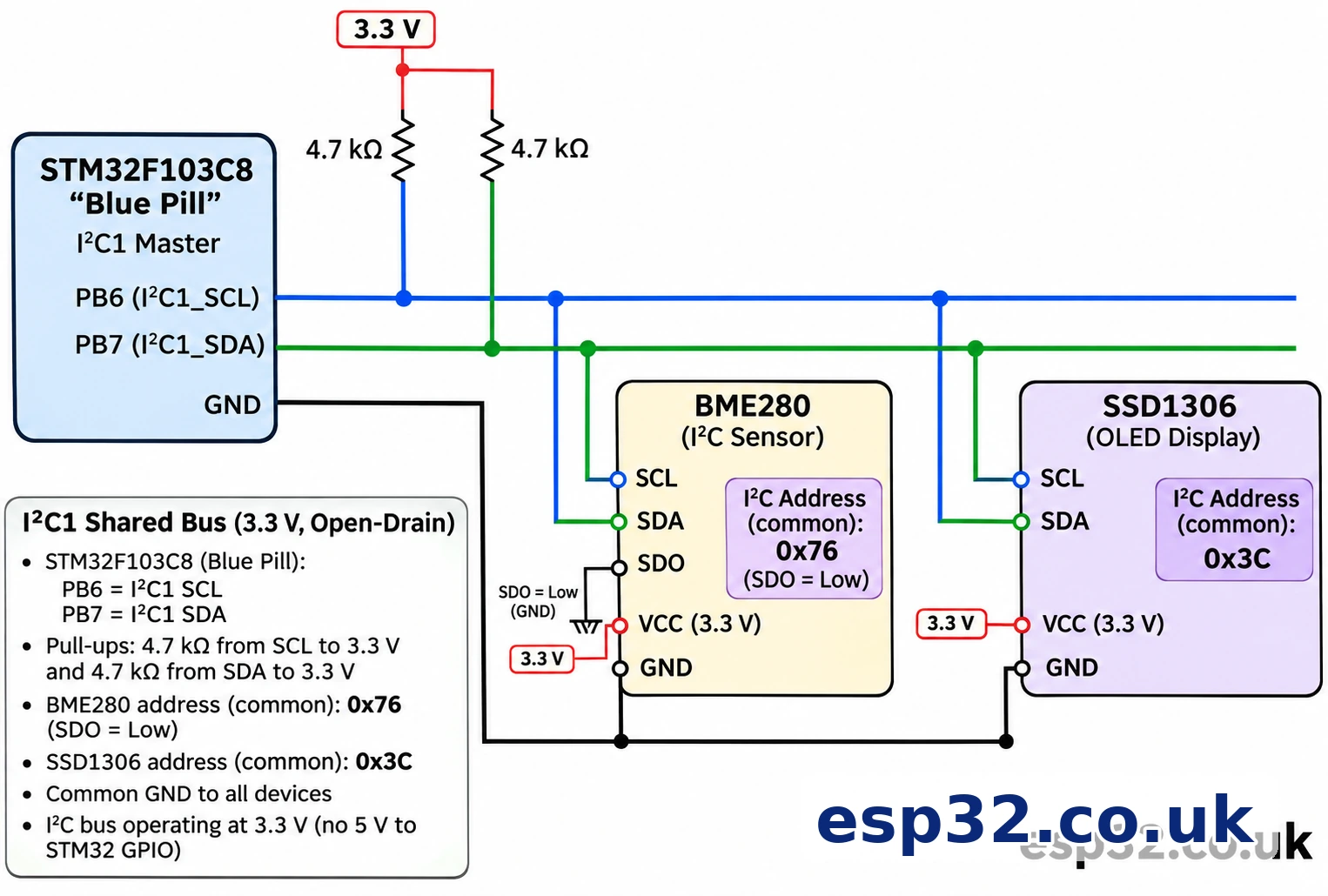
| Blue Pill | BME280-style breakout | Reason |
|---|---|---|
| PB6 / I2C1_SCL | SCL or SCK (I²C clock) | Shared clock line |
| PB7 / I2C1_SDA | SDA or SDI (I²C data) | Shared data line |
| GND | GND | Common electrical reference |
| Verified 3.3 V supply | Board 3V3/VCC as specified | Supply and logic voltage |
| 3.3 V through 4.7 kΩ | SCL, if not already pulled up | Allows the clock to rise |
| 3.3 V through a separate 4.7 kΩ | SDA, if not already pulled up | Allows the data line to rise |
| Sensor CSB (where present) | High, per BME280 I²C instructions | Chooses I²C rather than SPI on suitable modules |
| Sensor SDO (where present) | Ground for 0x76; VDDIO for 0x77 | Chooses the BME280’s 7-bit I²C address |
The phrase “if not already pulled up” matters. Many BME280 and OLED modules incorporate pull-ups on both lines. With power off, inspect the board or its schematic rather than blindly adding a second or third pair. When power is on and the bus is idle, both SCL and SDA should normally measure near the bus’s 3.3 V rail. A low line while everything should be idle is an immediate troubleshooting clue.
Keep the sensor wiring short and tidy. Do not assume the Blue Pill’s 3.3 V rail can supply an arbitrary collection of displays and sensors. Check the regulator’s capability, whether the board itself is USB-powered or externally powered, and whether any component draws substantial peak current. The SCL/SDA pull-ups should reference the bus’s valid logic rail, not simply the highest voltage available on a nearby module.
Why I2C does not use the UART’s crossed wires
USART wiring crosses the transmitter and receiver between devices. I²C is different: SCL connects to SCL and SDA connects to SDA on every participant. A BME280, an SSD1306 display and a small serial EEPROM can share the same two signal lines if their addresses are distinct, the bus speed is supported by all attached devices, and the power and pull-up arrangement are electrically compatible.
You do not need one pair of SCL/SDA pins per sensor. You do need a sensible total capacitive load and an address plan. Some device families have fixed addresses, some expose one or more address-select pins, and others are configured by hardware strapping or command sequences. A pair of identical fixed-address displays will conflict unless you add an appropriate multiplexer or put them on independent controllers.
Configure I2C1 in STM32CubeMX
Create a new STM32CubeMX project for STM32F103C8Tx. Keep SYS → Debug = Serial Wire so ST-LINK continues to use PA13/PA14. Enable I2C1 and leave its pins on PB6 and PB7 for this guide. Select I²C mode, a 100000 Hz target bus rate and 7-bit addressing. The hardware’s own address is not needed for normal master transactions, though CubeMX may still show an Own Address field with a default value.
| CubeMX setting | Suggested starting point | Explanation |
|---|---|---|
| MCU | STM32F103C8Tx | Matches genuine Blue Pill silicon variant |
| I2C1 mode | I2C | Standard I²C rather than SMBus |
| I2C1 SCL/SDA | PB6 / PB7 | Default AF open-drain mapping |
| Clock speed | 100000 Hz | Conservative, widely supported starting rate |
| Addressing mode | 7-bit | Most common sensor addresses are 7-bit |
| Dual addressing / general call | Disabled | Not needed for normal master-only sensor examples |
| No stretch | Disabled / allow stretching | Avoid unnecessarily rejecting legitimate device behaviour |
| SYS debug | Serial Wire | Keeps PA13/PA14 reserved for SWD |
| I2C interrupt / DMA | Disabled for initial polling | Add later only when needed and carefully configured |
Open the clock configuration and confirm the APB1 peripheral clock PCLK1 that feeds the F1 I²C controller. A typical Blue Pill configuration derives 72 MHz SYSCLK from an 8 MHz crystal and PLL ×9, then divides APB1 by two to get 36 MHz PCLK1. The HSE frequency is board-dependent, and the MCU does not require 72 MHz to use I²C. The generated setup must use the real clock rather than a number copied from an unrelated tutorial.
For an illustrative F1 100 kHz standard-mode calculation with PCLK1 = 36 MHz, the nominal I²C standard-mode CCR register count is 36,000,000 / (2 × 100,000) = 180. The TRISE setting for a 1 µs maximum rise-time assumption corresponds to 36 + 1 = 37 in this clock configuration. These values illustrate the reference manual’s mechanism; let CubeMX/HAL configure the actual registers and do not hard-code them unless you are intentionally implementing register-level drivers.
Fast mode caveat: The F103 family specifies limits and clock-accuracy qualifications for 400 kHz I²C. The 36 MHz PCLK1 example does not prove that a bus will deliver precisely 400 kHz; ST’s datasheet notes additional PCLK1 requirements for reaching the maximum fast-mode rate. Start at 100 kHz, validate the waveform and module, and increase speed only when the full bus is qualified. Faster is not automatically more robust.
The 7-bit address shift that causes so many failures
Suppose a sensor advertises address 0x76. That is usually the seven-bit device address, without the read/write bit. On the I²C wire, the controller transmits an eight-bit address byte by appending the R/W bit: 0xEC for a write phase and 0xED for a read phase.
In the classic STM32F1 HAL API, the DevAddress argument expects the seven-bit address left-shifted by one. Use:
#define BME280_ADDR_7BIT   0x76U
#define BME280_ADDR_HAL    (BME280_ADDR_7BIT << 1)

HAL_StatusTypeDef status = HAL_I2C_IsDeviceReady(
    &hi2c1, BME280_ADDR_HAL, 3, 100
);
Do not shift a value that has already been expressed in eight-bit wire format. Some reference material uses 0xEC as an “I²C address” because it is showing the transmitted write byte rather than the actual seven-bit identity. When migrating examples from Arduino Wire, Linux i2c-tools or another driver, inspect the API contract instead of blindly reusing the numeric value.
| 7-bit device address | HAL DevAddress argument | Wire address byte, write | Wire address byte, read |
|---|---|---|---|
0x3C | 0x78 | 0x78 | 0x79 |
0x50 | 0xA0 | 0xA0 | 0xA1 |
0x68 | 0xD0 | 0xD0 | 0xD1 |
0x76 | 0xEC | 0xEC | 0xED |
0x77 | 0xEE | 0xEE | 0xEF |
These examples are address arithmetic, not proof that a particular display or sensor uses that address. The board’s address-select straps, silicon identity and documentation determine which devices respond. The R/W bit is managed by the peripheral/HAL; do not OR it manually when calling ordinary HAL_I2C_Mem_Read() or HAL_I2C_Master_Transmit().
A simple I2C bus scanner in HAL
An address scanner is a useful first test because it distinguishes wiring problems from an incorrectly configured sensor library. The scanner below probes the legal 7-bit range 0x08–0x77 and logs responding addresses over USART1. Reserved values outside that range are deliberately not scanned. This example presumes hi2c1 has been initialised and that a separate 3.3 V USB-UART adapter has been configured as shown in our STM32 UART tutorial on esp32.co.uk/.
#include "main.h"
#include <stdio.h>
#include <string.h>

extern I2C_HandleTypeDef hi2c1;
extern UART_HandleTypeDef huart1;

static void uart_log(const char *message)
{
    HAL_UART_Transmit(&huart1, (uint8_t *)message,
                      (uint16_t)strlen(message), 100);
}

static void i2c_scan_once(void)
{
    char line[64];
    unsigned found = 0;

    uart_log("Scanning I2C1 at 100 kHz...\r\n");
    for (uint8_t addr7 = 0x08; addr7 <= 0x77; ++addr7)
    {
        HAL_StatusTypeDef st = HAL_I2C_IsDeviceReady(
            &hi2c1, ((uint16_t)addr7 << 1), 2, 20);
        if (st == HAL_OK)
        {
            (void)snprintf(line, sizeof(line),
                           "I2C device: 0x%02X\r\n", addr7);
            uart_log(line);
            ++found;
        }
    }
    (void)snprintf(line, sizeof(line),
                   "Scan complete, %u responding address(es).\r\n", found);
    uart_log(line);
}
Call i2c_scan_once() once after MX_I2C1_Init() and MX_USART1_UART_Init() in your generated application’s main() or a user-code section that runs after the initialisation. It is intentionally not called from an interrupt. Expect a healthy scan to print one or more seven-bit addresses such as 0x76 or 0x3C. A scanner is not a universal authentication test: a device may be held in reset, require a hardware enable pin, use a different voltage, or be temporarily unavailable.
The scanner also takes time. It issues up to 112 address probes, and a disconnected bus can time out repeatedly. Keep it as a commissioning tool, not a tight loop that monopolises your product’s CPU or bus. If HAL_I2C_IsDeviceReady() returns HAL_BUSY because the physical bus is stuck, scanning more addresses is not the cure: first diagnose the low line or stale peripheral state.
Read a BME280 chip ID over I2C
Once an address responds, perform a register read that has an unambiguous meaning. On a genuine Bosch BME280, register 0xD0 returns a chip ID of 0x60. A closely related BMP280 generally reports 0x58. Low-cost marketplace listings sometimes confuse BMP280 and BME280; checking the ID is a more useful first step than assuming a printed module description is correct. The chip ID is not a substitute for provenance or a test of all sensor channels.
#include "main.h"

extern I2C_HandleTypeDef hi2c1;

#define BME280_I2C_ADDR   (0x76U << 1) // SDO tied low
#define BME280_ID_REG     0xD0U

static HAL_StatusTypeDef bme280_read_id(uint8_t *id)
{
    if (id == NULL) return HAL_ERROR;
    return HAL_I2C_Mem_Read(&hi2c1,
                            BME280_I2C_ADDR,
                            BME280_ID_REG,
                            I2C_MEMADD_SIZE_8BIT,
                            id, 1, 100);
}

/* In main(), after MX_I2C1_Init():
   uint8_t id = 0;
   if (bme280_read_id(&id) == HAL_OK && id == 0x60U) {
       // BME280 identified; now initialise its measurements.
   }
*/
HAL_I2C_Mem_Read() handles the register-address write phase and data read phase, including the appropriate repeated-start sequence. The I2C_MEMADD_SIZE_8BIT argument describes the register address width, not the physical I²C device address width. Use a 16-bit register-address setting only when the device actually uses 16-bit register addressing, such as many larger serial EEPROMs. Do not use HAL_I2C_Master_Receive() alone and expect a register-based sensor to know which register you intended to read.
If the result is 0x58, check that you are using a BMP280 rather than a BME280; the pressure and temperature register model is related, but humidity functionality is not the same. If the read returns an error, log HAL_I2C_GetError(&hi2c1), inspect the actual bus and try the alternative address 0x77 << 1 only if the sensor’s address strap can select it. Avoid interpreting a timeout as “sensor ID 0.”
Writing configuration registers correctly
Reading an ID shows that the device is present, but real measurement also needs sensor-specific configuration. The BME280 has control registers for humidity oversampling, measurement oversampling and operating mode. Its order-of-operations requirements should come from the Bosch datasheet: in particular, humidity oversampling settings take effect after a subsequent write to ctrl_meas. Avoid copying isolated register constants without understanding their bit fields.
This HAL example shows the mechanics of writing a register; the values and ordering are a small illustration, not a complete BME280 measurement driver:
static HAL_StatusTypeDef bme280_write_reg(uint8_t reg, uint8_t value)
{
    return HAL_I2C_Mem_Write(&hi2c1,
                             BME280_I2C_ADDR,
                             reg,
                             I2C_MEMADD_SIZE_8BIT,
                             &value, 1, 100);
}

/* Example: humidity oversampling x1, then enable temperature and
   pressure oversampling x1 in normal mode after checking the sensor.
   For a production driver, follow the Bosch reset, status, config,
   calibration-coefficient and compensation procedures.
*/
if (bme280_write_reg(0xF2U, 0x01U) != HAL_OK) Error_Handler();
if (bme280_write_reg(0xF4U, 0x27U) != HAL_OK) Error_Handler();
The 0xF2 register controls humidity oversampling and 0xF4 includes temperature/pressure oversampling plus mode bits. To convert raw readings into real °C, hPa or relative humidity, a BME280 application must retrieve factory calibration coefficients and apply the manufacturer’s compensation algorithm. Using an uncorrected 20-bit ADC result directly as a temperature is not valid.
Sharing the bus with an SSD1306 display
A common second device is an SSD1306 OLED module that responds at 0x3C (sometimes 0x3D depending on address selection and module version). The wiring remains shared: PB6 goes to both sensor SCL and display SCL; PB7 goes to both SDA pins; all devices have common ground; and pull-ups should be suitable for the combined bus. The display’s power and logic voltage must be verified separately. Some modules marked “5 V compatible” contain regulators or level shifting; others expose pull-ups to their VCC rail.
| Device example | Typical 7-bit address | Check before wiring |
|---|---|---|
| BME280 | 0x76 or 0x77 | SDO strap, CSB mode, breakout VCC, actual chip ID |
| SSD1306 I²C OLED | 0x3C or 0x3D | Actual controller and onboard voltage/pull-up circuit |
| 24xx serial EEPROM | Often 0x50–0x57 | Address straps, internal address width, write-cycle delays |
| DS3231 RTC | Usually 0x68 | Battery / power variant and bus voltage |
| I²C multiplexer | Varies by part | Downstream addresses and channel-selection register |
A bus scanner only proves that a slave ACKed its address. A screen with a responding 0x3C address can still remain blank if its controller, reset wiring, I²C data framing or contrast commands are wrong. Similarly, an EEPROM may ACK a write yet need milliseconds to complete its internal programming before the next access.
For an SSD1306, a software library normally sends commands with a control byte and follows the controller’s page/column addressing rules; it is not enough to feed it ASCII text. Use an established driver matched to the actual display controller and geometry (128×32 versus 128×64). Diagnose and confirm one device at a time, then combine them on the shared bus.
Choose I2C pull-up resistors and bus speed
The often-repeated “always use 4.7 kΩ” advice is a useful first approximation, not a physical law. I²C rise time is determined by the pull-up resistance and total bus capacitance. A first-order approximation for a standard RC rising edge is t_r ≈ 0.8473 × R_pullup × C_bus, measuring the transition from 30% to 70% of the supply. At 100 pF and 4.7 kΩ, this yields roughly 398 ns; at 200 pF it becomes roughly 797 ns. Standard-mode rise-time limits are more tolerant than fast-mode limits.
| Scenario | Useful starting consideration | What to verify |
|---|---|---|
| Short 100 kHz breadboard, one sensor | 4.7 kΩ each line to 3.3 V | Correct idle-high and clean edges |
| Several breakouts with onboard pull-ups | Measure / calculate parallel equivalent | Do not overburden slave sink-current capability |
| 400 kHz, small local PCB | Stronger pull-up may be needed | Rise time, pull-down current, clock timing and MCU requirements |
| Long jumper cable | Shorten wiring before raising speed | Capacitance, reflections, noise and ground reference |
| Mixed-voltage parts | Proper bidirectional level translation | Never raise an unprotected 3.3 V bus to 5 V |
With two 4.7 kΩ pull-ups in parallel per line, the equivalent is about 2.35 kΩ. Four in parallel yield about 1.175 kΩ. That changes the current when a device pulls the line low and can stress the weaker device’s guaranteed output-low rating. The best value depends on the total line capacitance, supply voltage and the I²C sink-current limits of every connected part.
If you have an oscilloscope, measure the time it takes SDA and SCL to rise. If not, a sensible practical strategy is to begin with 100 kHz, use short wires, ensure one deliberate set of pull-ups, and only move to 400 kHz if you have a real performance need. ST’s data for the F103 medium-density devices gives up to 1000 ns rise time in standard mode and 300 ns in fast mode; consult the precise conditions in the datasheet.
Interrupts, DMA and repeated-start behaviour
Polling is appropriate when sensor register reads are infrequent, small and tolerant of blocking latency. HAL_I2C_Mem_Read() and HAL_I2C_Mem_Write() are straightforward for an initial sensor driver. If your firmware must remain responsive while a transfer runs, the F1 HAL exposes interrupt and DMA transfer APIs, including HAL_I2C_Master_Transmit_IT(), HAL_I2C_Master_Receive_IT() and corresponding DMA versions. Register-based devices also have memory-operation APIs; check exactly which variants exist in the driver revision bundled with your project.
Do not assume that starting an interrupt or DMA operation immediately completes the transaction. You must keep the transmit buffer valid until completion, handle HAL_BUSY, enable the correct I²C event/error interrupts, and dispatch through HAL’s IRQ handlers. On STM32F1, interrupt and DMA I²C paths have historically required careful attention to event/error interrupt setup. The HAL source and its release notes are better references than a sketch taken from another MCU family.
For a read involving a register pointer followed by multiple data bytes, prefer an API that handles the repeated start correctly. Combining separate “write then read” operations can introduce a STOP between them, which may be acceptable for some devices and invalid for others. Always check the device-specific timing and framing requirement.
DMA is not a universal cure for slow I²C or malformed wiring. It moves bytes between the peripheral and RAM; it cannot compensate for a stuck line, a missing ACK, invalid power levels or an incompatible device address. Small sensors sampled a few times per second rarely need DMA. The extra state machine and error handling are justified mainly when transfers are frequent or your application has strict CPU-latency constraints.
The STM32F1 I2C errata you should know
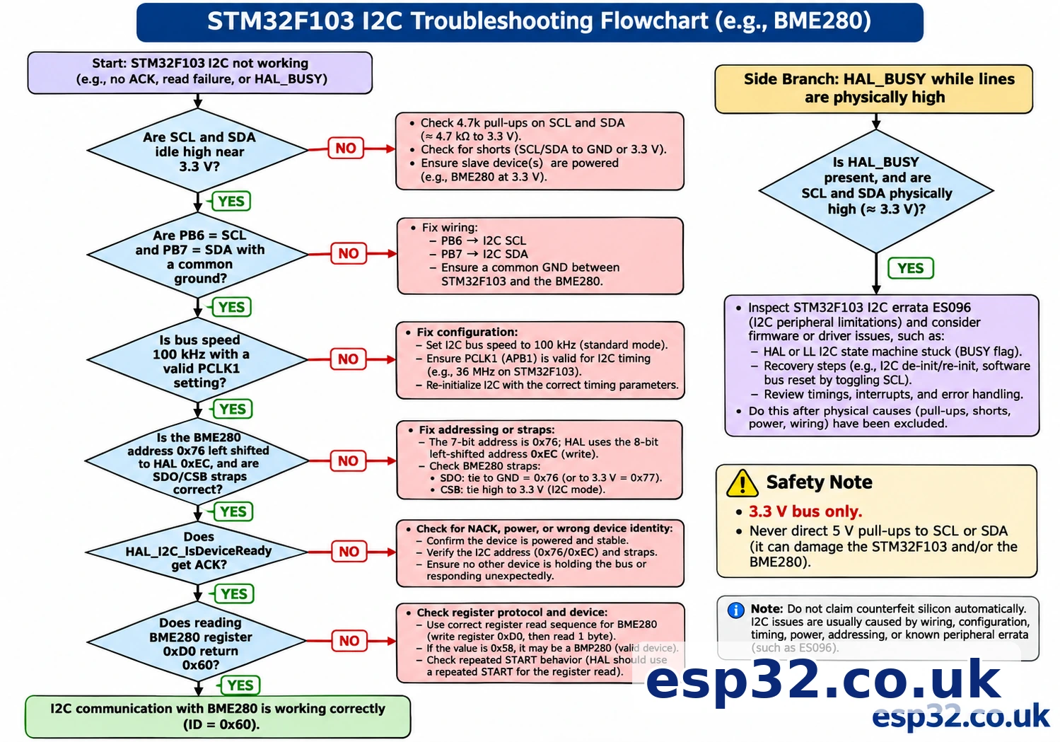
The STM32F103’s I²C peripheral has documented limitations. The official medium-density ES096 errata sheet discusses conditions involving wrong read data around certain receive/STOP sequences, handling unexpected STOP conditions, repeated-START timing and cases in which a low-level analog filter can cause an incorrect BUSY indication. The exact symptom and workaround are silicon- and condition-dependent; do not claim every F103 experiences the same failure.
If SCL and SDA are physically high but the I²C peripheral believes the bus is busy after reset, first rule out the ordinary causes: a connected slave holding SDA low, incorrect clock or GPIO initialization, or debugger/firmware interference. If the lines truly are high, the firmware is correct and you can reproduce the issue, consult the errata for your exact part revision, rather than applying an unverified generic “nine clocks fix.” A short, controlled GPIO-based bus-recovery sequence can help when a slave is holding data low, but it must check whether SCL is actually free and must not electrically fight another active master.
Similarly, if the final byte of a read is consistently corrupted under specific conditions, distinguish library versions and a timing bug from noisy wiring. ST’s HAL handles many hardware sequencing details, but it is still important to use a driver revision that supports your silicon and enables the correct I²C interrupt paths. A single HAL_I2C_ERROR_AF or HAL_TIMEOUT is a diagnostic clue, not proof that the MCU is faulty or counterfeit.
The source material is ST’s ES096 medium-density STM32F1 errata. It is particularly important if you’re turning a hobby breadboard into an unattended logger or industrial controller.
Troubleshooting: NACK, BUSY, no scanner results and wrong data
The most productive debugging method is to progress from electrical facts to software. With power off, check the wiring and pull-up connections. With power on and the bus idle, verify both lines sit near 3.3 V. Next confirm MCU pins, I²C peripheral, APB1 clock, address format and HAL error status. Only after those basics are correct should you investigate a suspect sensor or a complex hardware erratum.
| Symptom | Likely causes | First practical check |
|---|---|---|
| Scanner finds nothing | SCL/SDA swapped, no pull-ups, no sensor power, wrong pins | Confirm PB6/PB7, idle-high and common ground |
HAL_ERROR / NACK | Wrong address shift, wrong SDO strap, chip not ready | Log HAL error bits; probe 0x76 << 1 versus 0x77 << 1 appropriately |
HAL_BUSY before any data | SDA held low, startup race, stale peripheral state | Check the actual voltage on both lines before calling HAL |
| Clock pulses but no ACK | Wrong device address, powered-down target, unsuitable logic level | Check part number, CSB/SDO and address byte on a logic analyser |
| ID read returns 0xFF or 0x00 | Wrong register framing, absent sensor, stale buffer | Confirm HAL_OK, then examine register-address transaction |
| Works with one module, fails with two | Duplicate addresses, strong parallel pull-ups, power overload | Disconnect one module; inspect total pull-up strength |
| Works at 100 kHz but not 400 kHz | Slow rise, excessive capacitance or clock limits | Reduce cable length; measure edges; stay at 100 kHz if needed |
| Two-byte reads intermittently corrupt | Receive timing, bus noise, driver/silicon errata | Compare HAL version and ST’s ES096 conditions |
| SCL held low unexpectedly | A slave stretching clock or physical short | Check which device is holding it and its required timing |
| OLED ACKs but stays blank | Controller or init commands wrong | Validate the display driver’s exact controller and geometry |
A practical sequence is to run a single sensor at 100 kHz, read the ID register, then run the scanner, then enable the second device. Capture a few bytes on a logic analyser if available. In particular, watch for a START, the eight-bit address byte, the ACK bit and a STOP or repeated START. “No device found” becomes much easier to diagnose when you know whether the clock and address bytes appeared at all.
A production-friendly I2C driver design
A working demonstration should eventually become a predictable driver. Store the seven-bit address in your own configuration so you can switch between board variants, then shift at the HAL boundary in exactly one place. Use a function for a short register read, a function for a register write, and a clear error reporting strategy that distinguishes bus error, ACK failure, timeout and device identity mismatch.
Keep interrupts short. Avoid blocking serial output from an I²C callback. Use finite timeouts; don’t let a disconnected sensor lock the entire application forever. If the project runs unattended, add retry logic with a bounded backoff, fault counters and a way to signal that sensor readings are invalid rather than silently presenting stale values as current measurements.
Think carefully about startup order. The Blue Pill’s power rail must be stable before you access its I²C controller. A module with its own slower power sequence may not ACK immediately. Some devices need a brief delay after reset or a register command before making fresh measurements. Conversely, waiting an arbitrary large delay on every read is usually inefficient; use the actual busy/status flags and data-ready timing specified for the target device.
Document the breakout version, voltage rails, pull-up locations, bus speed, HAL release and MCU revision. These details are essential when a sensor project works perfectly on a desk and fails when installed inside an enclosure. A transparent, reproducible setup is more valuable than a schematic that looks attractive but does not identify the actual electrical constraints.
Frequently asked questions
Can I use PB8 and PB9 instead of PB6 and PB7?
Yes. The STM32F103 supports I2C1 remapping to PB8 (SCL) and PB9 (SDA). You must enable the peripheral remap in CubeMX/AFIO and ensure those pins are not used for other purposes. Merely moving the wires without changing the MCU configuration will not work.
Does the Blue Pill have built-in I2C pull-up resistors?
Do not rely on the Blue Pill board to provide a complete, correct external I²C pull-up arrangement. Some attached breakout modules include their own resistors. For a reliable design, identify the actual pull-up paths and ensure SCL/SDA rise to the intended 3.3 V bus voltage when idle.
Is 0xEC the same thing as I2C address 0x76?
0x76 is the seven-bit sensor identity. 0xEC is the corresponding eight-bit write address byte, which includes the R/W bit at its least-significant position. Classic STM32F1 HAL APIs expect 0x76 << 1, so the DevAddress argument is 0xEC in that case. The read/write direction is handled separately by HAL.
Can I power a 5 V OLED module while using 3.3 V I2C?
Only if the actual module schematic explicitly supports the voltage arrangement, including its bus pull-ups and any level shifting. A module labelled “5 V compatible” may be safe because it contains translation, or it may expose 5 V pull-ups that are not appropriate for this bus. Inspect before connecting; use a suitable bidirectional level shifter when required.
What is the correct speed for an STM32F103 I2C sensor?
100 kHz is an excellent initial choice. The device supports faster I²C configurations under the datasheet’s timing and clock requirements, but the full bus must also meet rise-time, capacitance and signal-integrity limits. Do not assume a 400 kHz setting guarantees a 400 kHz waveform at every PCLK1 configuration.
Does DMA make an I2C sensor more accurate?
No. DMA reduces CPU involvement during data movement; it does not improve the sensor’s analog measurement accuracy or fix poor I²C signals. A small BME280 reading every second usually works well with polling; DMA is more useful for larger or more frequent transfers.
Can two BME280s use the same I2C address?
Not on the same simultaneously active bus without some form of separation. Depending on SDO selection, two BME280s can normally be assigned 0x76 and 0x77. If both must use the same address, choose independent I²C controllers or a suitable mux, and review the target board’s connections.
Why does my Blue Pill scanner find devices but the sensor library still fail?
The bus and address phase are working, but the device may require a particular register protocol, reset sequence, measurement mode, register-width setting or compensation algorithm. Confirm the chip ID and compare your transactions with the manufacturer’s datasheet. A scanner is the first test, not the final one.
Final checklist before building the next sensor project
- Verify the exact STM32F103C8 and sensor breakout versions.
- Connect PB6 → SCL, PB7 → SDA, GND → GND, with suitable 3.3 V power and pull-ups.
- Start at 100 kHz with short wiring and only the intended pull-up network.
- Use 7-bit device addresses shifted one bit left at the F1 HAL interface.
- Read a known device-identification register before implementing measurements.
- Enable interrupt/DMA transfers only once ordinary polling works and the callbacks/error paths are understood.
- Consult the ES096 I²C errata if bus, BUSY or read-sequence faults remain reproducible after electrical checks.
- Confirm both electrical correctness and firmware protocol correctness before adding more devices.
In this esp32.co.uk/ article, the governing principle is simple: an I²C interface is only as reliable as its bus wiring, pull-ups, address handling and transfer sequence. Once those are correct, the STM32F103 Blue Pill is perfectly capable of reading a sensor, driving a display and coordinating several low-speed peripherals on the same two lines.
Technical references and further reading
- ST RM0008 — STM32F1 reference manual — I²C controller registers, timing and I2C1 remapping.
- ST DS5319 — STM32F103x8/xB datasheet — electrical characteristics and I²C rise-time limits.
- ST ES096 — F103 medium-density silicon errata — I²C receive and BUSY-related limitations.
- ST STM32F1 HAL I²C driver — documented HAL address format and transfer APIs.
- Bosch BME280 datasheet — chip ID, address select, control registers and compensation.
- STM32 UART tutorial — esp32.co.uk/ — serial logging for scanner output.
- STM32 GPIO tutorial — esp32.co.uk/ — debugging and first CubeMX project.