SPI is the next useful step after learning GPIO, UART, ADC and I²C on the STM32 Blue PillPriceAliExpress price. It gives the microcontroller a direct, clocked connection to sensors, displays and other peripherals, with enough bandwidth to move more than occasional register values. The wiring is straightforward, but successful communication depends on agreeing about clock edges, chip select and exactly which bytes belong to one transaction.
This tutorial builds that understanding around an STM32F103C8T6PriceAliExpress price, SPI1 and the STM32PriceAliExpress price HAL. We will start with a loopback test, read the identity register of an ST LIS3DH accelerometer, examine how a display changes the transaction structure, and then move the sensor transfer to DMA. The examples use a deliberately modest clock so you can see what is happening before attempting higher speeds.
The code is intended for a CubeMX-generated STM32CubeF1 project. It is instructional application code, rather than a complete downloadable IDE project or a claim of testing on physical hardware. Keep the generated clock, interrupt and peripheral initialization functions, and add the examples in the designated user-code areas. The sections below explain the settings on which that code depends.

What SPI actually transfers
In a conventional four-wire SPI connection, the controller generates SCK, sends data on MOSI and receives data on MISO. A separate chip-select signal tells a peripheral when to pay attention. Older documentation calls these signals master out slave in and master in slave out. On a sensor, the same pins may be marked SDI and SDO: connect the STM32 output to the sensor input, and the sensor output to the STM32 input.
Sending and receiving happen together. Every eight clock pulses in an eight-bit configuration shift one byte out and one byte in. A sensor register read therefore requires the STM32 to transmit something while the requested value comes back. The outgoing byte can be a dummy value if the peripheral protocol permits it. A receive buffer also contains whatever arrived during the command phase; that first byte is generally not the register value you wanted.
SPI does not supply an I²C-style address or acknowledgement mechanism. Selecting a device is usually a matter of asserting its CS pin, commonly active low. A function returning HAL_OK tells you that the MCU completed its side of the transfer. It does not establish that the sensor exists or understood the command. Reading a fixed identification value is a much more useful first functional test.
There is also no universal SPI register protocol. One peripheral may use a read bit in the command byte, another may require an opcode and a three-byte address, and a display may distinguish commands from pixel data using a separate pin. Treat each device datasheet as the definition of the bytes on the bus. Do not reuse an I²C address, add an address shift, or assume that a register read automatically increments.
If those distinctions are unfamiliar, the earlier STM32 I²C tutorial provides a useful comparison. SPI needs more select wires as the number of devices grows, but it avoids shared address conflicts and makes long transfers relatively simple to organize.
Hardware, voltage and the SPI1 pin map
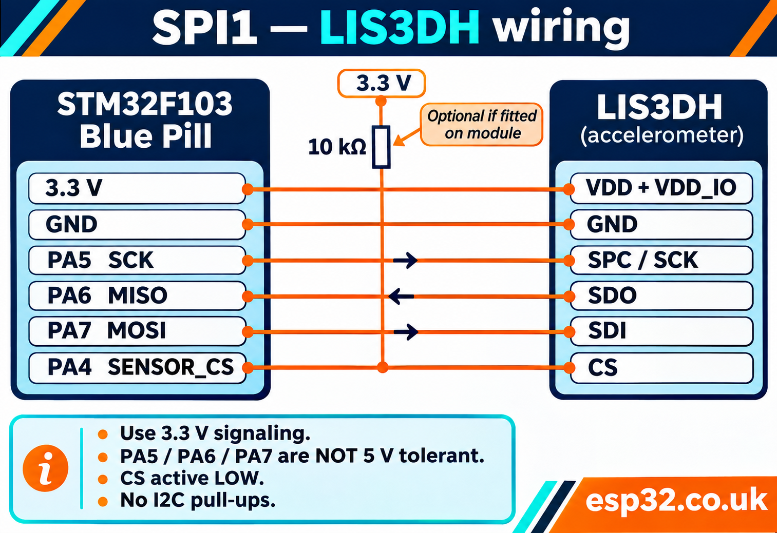
Use a Blue Pill with an STM32F103C8T6, an ST-LINK-compatible debugger, short jumper wires and a peripheral whose logic operates at 3.3 V. A logic analyzer is helpful but optional. For the sensor example, choose an LIS3DH breakout that exposes its four-wire SPI signals. Confirm the module schematic: a board intended only for I²C may strap CS high or hide the signal you need.
The default SPI1 mapping is PA5 for SCK, PA6 for MISO and PA7 for MOSI. PA4 can be the hardware NSS pin, but here it is an ordinary GPIO output called SENSOR_CS. That choice gives the application explicit control over the entire command-and-data transaction. It also leaves the tutorial independent of the behavior of hardware NSS between transfers. The assignments are listed in ST’s STM32F103x8/xB datasheet, in the pin-definition table.
| Blue Pill signal | LIS3DH breakout signal | Purpose |
|---|---|---|
| 3.3 V | VDD and VDD_IO as required by module | Power and logic supply |
| GND | GND | Common reference |
| PA5 | SPC or SCK | Clock from STM32 |
| PA6 | SDO | Data from sensor |
| PA7 | SDI | Data to sensor |
| PA4 | CS | Active-low sensor selection |
PA5, PA6 and PA7 are not marked FT in the device pin table. Do not apply 5 V to these pins. A module advertised as accepting a 5 V supply may contain a regulator without including suitable signal-level translation. Check both the power input and the electrical levels at its SPI header. For this setup, use 3.3 V signaling throughout. The STM32 GPIO voltage guide explains why a family-wide claim about tolerant pins is not enough.
Disconnect power while moving wires, establish a shared ground and avoid powering the board simultaneously from competing sources. An ST-LINK target-voltage connection can be a sensing input rather than a power output, depending on the debugger. Follow its documentation. Do not assume every clone debugger labels its connector correctly, and do not allow an externally powered peripheral to drive an unpowered MCU through the signal pins.
Place a pull-up, typically 10 kΩ to the peripheral’s 3.3 V logic supply, on each active-low CS if the module does not already provide one. This keeps the peripheral deselected while the STM32 resets and its GPIO pins are inputs. SPI clock and data lines do not need the I²C-style pair of bus pull-ups. Use the peripheral manufacturer’s decoupling recommendations, and power a display backlight from an appropriate supply or driver rather than directly from a GPIO.
Clock modes and a sensible starting speed
Clock polarity, CPOL, sets the idle clock level. Clock phase, CPHA, chooses whether sampling occurs on the first or second clock transition of a bit. Both ends must agree. A transfer may produce plausible-looking values even with the wrong phase, particularly on short wires at low speed, so a few nonzero bytes are not sufficient verification.
| SPI mode | CPOL | CPHA | Idle clock | Sampling edge |
|---|---|---|---|---|
| Mode 0 | 0 | 0 | Low | Rising |
| Mode 1 | 0 | 1 | Low | Falling |
| Mode 2 | 1 | 0 | High | Falling |
| Mode 3 | 1 | 1 | High | Rising |
The LIS3DH example uses mode 3: CPOL high and sampling on the second edge. ST’s LIS3DH datasheet, section 6.2, describes a clock stopped high and data captured on its rising edge. Configure MSB first and eight-bit data frames. A different sensor or display can require a different mode; the table helps translate its timing diagram into CubeMX settings.
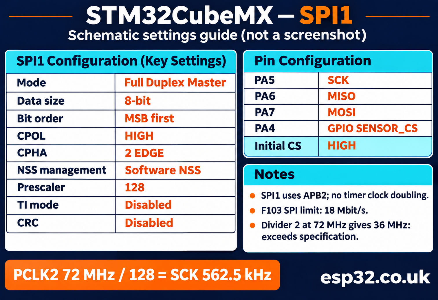
SPI1 is clocked from APB2. With PCLK2 at 72 MHz, a prescaler of 128 produces 562.5 kHz. Prescalers of 64, 32, 16, 8 and 4 would produce 1.125, 2.25, 4.5, 9 and 18 MHz respectively. The APB timer clock doubling rule does not apply to SPI. Always use the actual peripheral clock shown in your clock configuration, rather than assuming it equals the CPU clock.
ST specifies these STM32F103 devices with SPI capability up to 18 Mbit/s. A selectable divider of two is not permission to run this device at 36 MHz. The allowable bus speed is bounded by the MCU electrical specifications, the peripheral timing requirements and the quality of the wiring. The LIS3DH itself has its own SPI timing limits. Leave the initial divider at 128 while proving the circuit, then increase speed only when repeated transfers remain reliable.
At 562.5 kHz, a two-byte transaction takes about 28.4 microseconds of clocking, excluding software overhead and CS gaps. That is already fast enough for an identity check. Raising the clock prematurely makes setup-time, grounding and probe problems harder to distinguish from software mistakes.
Configure the project in CubeMX
Select the actual STM32F103C8 package when creating the project. Keep Serial Wire debugging enabled so PA13 and PA14 remain available for SWD. Enable SPI1 as full-duplex master, with software NSS management. Confirm that the selected pins are PA5, PA6 and PA7; do not enable SPI1 remapping for this circuit. A remapped project can compile perfectly while generating its clock on another pin.
Set the data size to eight bits, first bit to MSB, clock polarity to high and phase to the second edge. Choose the 128 prescaler, disable TI mode and disable hardware CRC for these peripheral examples. Configure PA4 as a push-pull GPIO output with an initial high level and give it the user label SENSOR_CS. CubeMX should then generate SENSOR_CS_Pin and SENSOR_CS_GPIO_Port in main.h.
Configure the clock tree explicitly. If your board has a verified 8 MHz external crystal, the usual PLL arrangement can provide 72 MHz SYSCLK, 72 MHz APB2 and 36 MHz APB1. Do not select that external oscillator merely because a board resembles a Blue Pill; inspect the hardware. An internal-clock configuration also works for this SPI exercise if the divider calculation is updated to match its PCLK2.
Generate the project and inspect the initialization order in main. HAL_Init and SystemClock_Config should precede GPIO and SPI initialization. The generated MSP initialization must enable the SPI1 and GPIO clocks and configure SCK/MOSI as alternate-function push-pull, with MISO as an input. STM32F1 GPIO configuration differs from newer STM32 families, so copying a modern alternate-function-number setup is not appropriate here.
The essential SPI fields should look like this inside the generated initialization function. Use CubeMX as the owner of these settings and compare its output; avoid maintaining a second conflicting copy of MX_SPI1_Init in user code.
hspi1.Instance = SPI1;
hspi1.Init.Mode = SPI_MODE_MASTER;
hspi1.Init.Direction = SPI_DIRECTION_2LINES;
hspi1.Init.DataSize = SPI_DATASIZE_8BIT;
hspi1.Init.CLKPolarity = SPI_POLARITY_HIGH;
hspi1.Init.CLKPhase = SPI_PHASE_2EDGE;
hspi1.Init.NSS = SPI_NSS_SOFT;
hspi1.Init.BaudRatePrescaler = SPI_BAUDRATEPRESCALER_128;
hspi1.Init.FirstBit = SPI_FIRSTBIT_MSB;
hspi1.Init.TIMode = SPI_TIMODE_DISABLE;
hspi1.Init.CRCCalculation = SPI_CRCCALCULATION_DISABLE;
hspi1.Init.CRCPolynomial = 7;
if (HAL_SPI_Init(&hspi1) != HAL_OK) {
    Error_Handler();
}
Prove the STM32 side with loopback
Before connecting a sensor, temporarily join PA7 to PA6, leaving PA5 unconnected to any peripheral and keeping every CS high. The STM32 will receive the bits it sends. This checks the GPIO mapping, clock generation, data size and basic HAL path without depending on a device-specific command. Disconnect all other drivers from MISO first so this jumper cannot connect two outputs together.
Add the following after the generated initialization calls. Include string.h in a user include area for memcmp. Inspect the result in the debugger; no printf routing is required. A passing loopback establishes a useful starting point, but it cannot prove that a real peripheral supports the selected mode or voltage. Remove the loopback jumper before connecting the sensor.
/* User includes: #include <string.h> */
uint8_t loop_tx[] = {0x00, 0xFF, 0xA5, 0x3C};
uint8_t loop_rx[sizeof loop_tx] = {0};
HAL_StatusTypeDef loop_status = HAL_SPI_TransmitReceive(
    &hspi1, loop_tx, loop_rx, sizeof loop_tx, 20);
volatile uint8_t loop_pass = (loop_status == HAL_OK) &&
    (memcmp(loop_tx, loop_rx, sizeof loop_tx) == 0);
(void)loop_pass;
If the receive bytes are all zero, inspect the physical connection and the generated MISO configuration. If no SCK is present, check that execution reaches the call and that the SPI peripheral clock is enabled. When using an analyzer, attach its ground close to the board ground and configure its decoder for mode 3, eight bits and MSB first. Triggering on CS is useful for a peripheral transaction, but this loopback deliberately does not assert a CS.
The GPIO tutorial is a useful place to revisit generated pin labels and user-code regions. For reporting values over a serial terminal later, follow the UART tutorial rather than assuming that printf automatically reaches a USB connector.
Read a real LIS3DH identification register
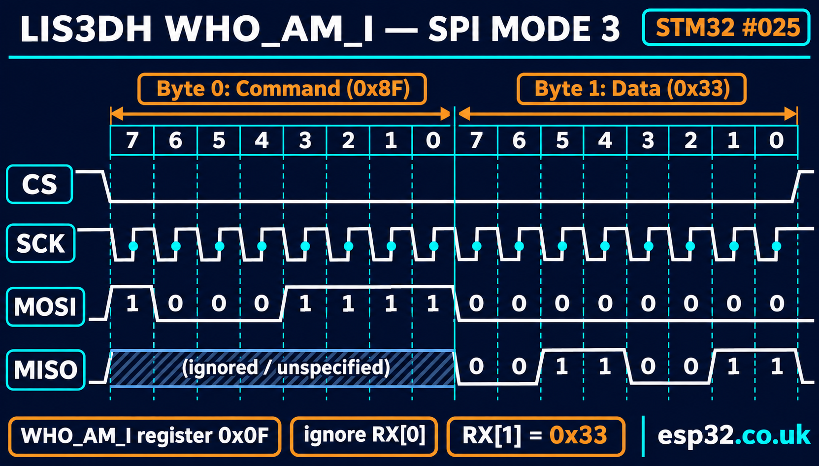
Restore the sensor wiring and keep mode 3. The LIS3DH WHO_AM_I register is at address 0x0F and returns 0x33. A single-register SPI read sets command bit 7 and leaves the multiple-byte increment bit clear, giving command 0x8F. Send a dummy byte after that command. The meaningful identity value is the second received byte, because the first eight clocks carried the command.
Keep CS low across both bytes. Raising it between the command and the dummy byte ends the transaction and makes the second transfer a new command. This is why a software-controlled select pin is useful: the transaction boundary belongs to the device protocol, which may span several calls or several buffers.
Put these functions in a user-code section at file scope in main.c, where hspi1 is already defined, or in a separate module that includes main.h and declares the generated SPI handle. They share the same CS label configured earlier. Call them from ordinary foreground code after initialization, rather than from a high-priority interrupt.
static HAL_StatusTypeDef lis_read(uint8_t reg, uint8_t *value)
{
    if (value == NULL) return HAL_ERROR;
    uint8_t tx[2] = {(uint8_t)(0x80U | (reg & 0x3FU)), 0x00};
    uint8_t rx[2] = {0};
    HAL_GPIO_WritePin(SENSOR_CS_GPIO_Port, SENSOR_CS_Pin, GPIO_PIN_RESET);
    HAL_StatusTypeDef st = HAL_SPI_TransmitReceive(&hspi1, tx, rx, 2, 20);
    HAL_GPIO_WritePin(SENSOR_CS_GPIO_Port, SENSOR_CS_Pin, GPIO_PIN_SET);
    if (st == HAL_OK) *value = rx[1];
    return st;
}

static HAL_StatusTypeDef lis_write(uint8_t reg, uint8_t value)
{
    uint8_t tx[2] = {(uint8_t)(reg & 0x3FU), value};
    uint8_t rx[2];
    HAL_GPIO_WritePin(SENSOR_CS_GPIO_Port, SENSOR_CS_Pin, GPIO_PIN_RESET);
    HAL_StatusTypeDef st = HAL_SPI_TransmitReceive(&hspi1, tx, rx, 2, 20);
    HAL_GPIO_WritePin(SENSOR_CS_GPIO_Port, SENSOR_CS_Pin, GPIO_PIN_SET);
    return st;
}

/* Foreground, after peripheral initialization and sensor power-up: */
/* uint8_t identity = 0;
   if (lis_read(0x0F, &identity) != HAL_OK || identity != 0x33) {
       Error_Handler();
   }
*/
Both functions release CS on a timeout or error as well as on success. Their receive buffers also drain the incoming bytes during a write. The 20 ms timeout is deliberately generous for two bytes at the initial speed, while still bounding the foreground wait. In a product, report the error, record HAL_SPI_GetError and recover the bus before retrying; repeatedly calling a fatal handler is only a simple demonstration policy.
Allow the sensor’s specified power-up interval before the first access. HAL_GPIO_WritePin provides no portable guarantee of a particular nanosecond setup or hold delay. At this conservative clock the ordinary software sequence is a practical starting point, but inspect the device timing requirements if you optimize GPIO accesses or raise the speed. Use a timer or another measured mechanism if you need a defined short delay.
Move from identity to acceleration data
An identity register can be readable while the sensor remains in its default power-down measurement state. For a simple LIS3DH measurement setup, CTRL_REG1 at 0x20 can be written with 0x57 to select 100 Hz normal operation with all three axes enabled. CTRL_REG4 at 0x23 can be written with 0x88 to enable block data update and high-resolution mode at ±2 g, while retaining four-wire SPI and the default byte order. Check both writes and read the settings back.
Wait for startup settling as specified for the chosen operating mode, then poll the data-ready status or use a properly configured interrupt. A successful SPI transaction is unrelated to whether a new acceleration sample is available. Reading in a tight loop can simply return the same physical sample many times, while reading too slowly can discard intermediate samples unless you deliberately use the FIFO.
The axis outputs occupy six consecutive registers beginning at OUT_X_L, 0x28. A burst-read command is 0xE8: read plus auto-increment plus the starting address. Transmit that command followed by six dummy bytes and receive seven bytes under one CS assertion. Ignore receive byte zero, then combine low and high bytes for X, Y and Z. The command format is specific to LIS3DH; it must not become a universal sensor-read helper.
In high-resolution mode, the useful signed value is left-justified in the 16-bit register pair. After forming a signed 16-bit value, divide by 16 to obtain the 12-bit count. At the ±2 g setting, the nominal sensitivity is 1 mg per count. Preserve the sign when converting, and do not treat the full unshifted 16-bit number as a directly scaled measurement. Calibration, mounting orientation and sensor tolerances still matter even after the byte format is correct.
For a stationary board, gravity gives a useful plausibility check: the vector magnitude should be approximately one g, with the dominant axis changing when you turn the board. It is not a precision calibration. If one axis flips sign unexpectedly, check the byte order and signed conversion before blaming SPI. Compare with the earlier ADC tutorial for the distinction between moving a numeric result and establishing a trustworthy physical measurement.
How a display changes the transaction
A display often receives long bursts rather than a command and one returned register. Many modules provide SCK, MOSI, CS, a data/command pin and reset. Some omit MISO entirely because the application only writes. Others label the serial pins SCL and SDA even though the interface is SPI. Inspect the actual controller and module interface configuration before connecting an I²C-style circuit.
As a concrete transport example, consider an SPI-connected SSD1306 module that is already configured for its four-wire serial interface. Reserve PB0 as DISPLAY_CS, PB1 as DISPLAY_DC and PB10 as DISPLAY_RST, all GPIO outputs. Keep SENSOR_CS high while addressing the display. Set DISPLAY_CS high initially and follow the display module’s reset and power sequence. The Solomon Systech SSD1306 datasheet, section 8.1.3, explains its D/C-controlled four-wire interface. Use the panel-specific initialization; the transport below does not substitute for that sequence.
The helper sends a command block with D/C low or a data block with D/C high. Its clock polarity and phase must first be configured for the display’s documented interface, with SPI idle and both selects high. Do not run it while the sensor’s DMA operation owns the bus. The helper is a transport example, not a complete display driver, and these extra pin labels must exist in the generated project before it compiles.
static HAL_StatusTypeDef display_send(uint8_t *bytes,
                                      uint16_t count, GPIO_PinState dc)
{
    if (bytes == NULL || count == 0) return HAL_ERROR;
    HAL_GPIO_WritePin(DISPLAY_DC_GPIO_Port, DISPLAY_DC_Pin, dc);
    HAL_GPIO_WritePin(DISPLAY_CS_GPIO_Port, DISPLAY_CS_Pin, GPIO_PIN_RESET);
    HAL_StatusTypeDef st = HAL_SPI_Transmit(&hspi1, bytes, count, 100);
    HAL_GPIO_WritePin(DISPLAY_CS_GPIO_Port, DISPLAY_CS_Pin, GPIO_PIN_SET);
    return st;
}
A 128 by 64 monochrome framebuffer uses 1,024 bytes. A 240 by 320 RGB565 framebuffer needs 153,600 bytes, which exceeds the STM32F103C8’s 20 KB SRAM before accounting for anything else. For a color display, use scanlines, tiles or smaller rectangles. At 9 MHz, moving 1,024 bytes requires approximately 0.91 ms of clocking, while 153,600 bytes takes about 137 ms before commands and software overhead. These calculations help decide whether a framebuffer or DMA will solve your actual bottleneck.
Do not carry an SSD1306 command sequence into an ST7789 or ILI9341 driver. Color controllers have different initialization, pixel formats, address windows and reset requirements. Begin with a known controller-specific initialization and one solid-color rectangle, then add text or graphics. A lit backlight proves only that the backlight circuit has power.
Share the bus without mixing transactions
Several peripherals can share SCK and MOSI, and they can share MISO when every deselected device genuinely releases its output. Give each device its own CS. Some breakout boards include level translators or buffers that continue driving MISO even with CS high. That hardware prevents straightforward sharing and may require a different module, an isolation buffer or a separate SPI peripheral.
Treat bus ownership as covering configuration, CS assertion, every byte and final deselection. If the sensor uses mode 3 and the display needs another mode, finish the current transfer, confirm the bus is idle, keep all selects high, and reconfigure the SPI handle before selecting the next device. Restore the correct configuration before returning to the sensor. A peripheral driver should not silently assume that another driver left the clock settings unchanged.
In a bare-metal main loop, a single owner can serialize these calls. Under an RTOS, use a mutex or a dedicated SPI service task and hold ownership until an asynchronous transfer has actually completed. An interrupt that starts another transaction halfway through a sensor burst can corrupt both devices even when each driver works perfectly on its own. HAL’s busy state helps detect some overlap, but it does not replace application-level ownership across multiple calls.
Use DMA after blocking transfers work
DMA moves bytes between memory and the SPI data register while the CPU does other work. It does not increase the wire clock, interpret a sensor command or toggle your software CS. For a two-byte identity read the setup overhead is rarely worthwhile. A repeated sensor burst or a display block is a better candidate. First prove the same bytes with blocking HAL calls, then change the transfer mechanism.
For default SPI1 on this device, configure DMA1 Channel 2 for RX and DMA1 Channel 3 for TX. Select normal mode, peripheral increment disabled, memory increment enabled and byte alignment for peripheral and memory. Enable the relevant DMA interrupts and the SPI1 interrupt for error handling. The generated handlers must call HAL_DMA_IRQHandler for their linked handles and HAL_SPI_IRQHandler for hspi1. Initialize DMA before SPI so the MSP code can link its DMA handles correctly.
The next example reads the same identity register asynchronously. Place its static variables and functions at file scope. Call sensor_dma_start only from one foreground owner, then call sensor_dma_service frequently in the main loop. Do not call the blocking helpers, reconfigure SPI or start another user of the bus while dma_active is set. The public HAL completion callback is used rather than the raw DMA channel callback.
static uint8_t dma_tx[2] = {0x8F, 0x00};
static uint8_t dma_rx[2];
static volatile uint8_t dma_active, dma_event;
static uint32_t dma_started;
static volatile uint8_t dma_identity, dma_identity_valid;
static volatile uint32_t dma_last_error;

static HAL_StatusTypeDef sensor_dma_start(void)
{
    if (dma_active) return HAL_BUSY;
    dma_event = 0;
    dma_identity_valid = 0;
    dma_last_error = HAL_SPI_ERROR_NONE;
    dma_active = 1;
    dma_started = HAL_GetTick();
    HAL_GPIO_WritePin(SENSOR_CS_GPIO_Port, SENSOR_CS_Pin, GPIO_PIN_RESET);
    HAL_StatusTypeDef st = HAL_SPI_TransmitReceive_DMA(
        &hspi1, dma_tx, dma_rx, 2);
    if (st != HAL_OK) {
        /* Quiesce any partly armed DMA path before returning ownership. */
        (void)HAL_SPI_Abort(&hspi1);
        HAL_GPIO_WritePin(SENSOR_CS_GPIO_Port, SENSOR_CS_Pin, GPIO_PIN_SET);
        dma_active = 0;
    }
    return st;
}

void HAL_SPI_TxRxCpltCallback(SPI_HandleTypeDef *hspi)
{
    if (hspi == &hspi1 && dma_active) dma_event = 1;
}

void HAL_SPI_ErrorCallback(SPI_HandleTypeDef *hspi)
{
    if (hspi == &hspi1 && dma_active) {
        dma_last_error = HAL_SPI_GetError(hspi);
        dma_event = 2;
    }
}

static void sensor_dma_service(void)
{
    if (!dma_active) return;
    uint8_t event = dma_event;
    if (event == 0 && (uint32_t)(HAL_GetTick() - dma_started) < 20U)
        return;
    if (event != 1) {
        if (event == 0) dma_last_error = HAL_SPI_ERROR_FLAG;
        (void)HAL_SPI_Abort(&hspi1); /* foreground recovery */
    }
    HAL_GPIO_WritePin(SENSOR_CS_GPIO_Port, SENSOR_CS_Pin, GPIO_PIN_SET);
    if (event == 1) {
        dma_identity = dma_rx[1];
        dma_identity_valid = (dma_identity == 0x33);
    }
    dma_active = 0;
}
The buffers are static because DMA continues after the start function returns. A local array on that function’s stack would no longer have a valid lifetime. Do not modify the outgoing buffer or consume the incoming buffer while the transfer is active. The STM32F103 has no data cache requiring the cache-maintenance procedures seen in some newer STM32 tutorials, but buffer ownership still applies.
Raw DMA transfer-complete means the programmed memory movement finished. Especially on a transmit path, the last bits can still be leaving the SPI shift register. ST’s STM32F1 HAL SPI driver performs transfer-closing checks before calling the public normal-mode completion callback. This example assumes that HAL behavior and releases CS later in the foreground. If you replace HAL with register code, implement the documented TXE/BSY completion sequence and bounded error handling yourself.
Keeping callbacks short also avoids printing or waiting inside an interrupt. The main-loop deadline catches a missing callback, but it depends on the foreground service continuing to run. If abort fails or the bus remains faulty, stop scheduling traffic and reinitialize the peripheral through a controlled recovery path before retrying. A production driver needs that explicit fault policy rather than treating every aborted transfer as successful.

Troubleshoot the signal before rewriting the driver
If every read returns 0xFF, first check whether MISO is disconnected or weakly pulled high. Verify CS reaches the sensor pin, the module is powered and its interface selection is correct. All-zero data can indicate a grounded or unpowered signal, but neither pattern identifies a fault uniquely. Measure the actual pins and check a known register rather than applying a software fix based only on a repeated byte value.
If the value is shifted or intermittently wrong, compare clock mode, bit order and frame size with the peripheral timing diagram. Decode mode 3 for this sensor and look for exactly sixteen clocks under one CS-low interval during the identity read. MOSI should contain 0x8F followed by 0x00; MISO’s second byte should be 0x33. The first MISO byte is unspecified for the application and should not be used as an error indication.
If communication works slowly but fails at a higher divider setting, shorten wires, improve the ground return and inspect clock ringing. Use appropriate GPIO output speed and consider modest source-series damping only after observing the signal and accounting for the electrical design. A logic analyzer reports interpreted logic transitions; an oscilloscope can reveal overshoot, slow edges or noise that the decoder hides. Do not assume an analyzer’s maximum sample rate guarantees reliable decoding near that rate.
If DMA starts but never completes, check the generated DMA channel assignments, NVIC enables, handler names and HAL handle links. Inspect whether the call returned HAL_OK before waiting for a callback. HAL_BUSY usually means ownership or a previous unfinished transfer needs attention. An overrun error points toward received data not being serviced in time or an incorrectly handled transfer path. Record the HAL error code before resetting the peripheral so the useful evidence is not lost.
If a final byte is truncated, inspect CS timing relative to the final clock edge. Releasing CS immediately after HAL_SPI_TransmitReceive_DMA returns is wrong because that return only confirms a successful start. If sharing breaks an otherwise working circuit, disconnect the second peripheral and test whether its MISO output really becomes high impedance when deselected. Recheck the mode restoration and select levels before changing DMA priorities.
ST’s RM0008 reference manual is the authority for the F1 SPI registers and DMA request mapping. AN5543 adds guidance across several SPI generations; features described for newer hardware are not automatically available on the F103. Consult the medium-density ES096 errata through ST’s STM32F103 documentation page for your device revision, especially when moving beyond this master-mode exercise.
Build the next project from verified transactions
Keep the successful loopback pattern, sensor identity check and analyzer capture with your project notes. They provide quick regression checks when adding a display, changing the clock tree or introducing an RTOS. Record the device mode, maximum tested clock, CS polarity and buffer ownership alongside each driver. Those small details are often what gets lost when a working experiment becomes a larger application.
The useful result is a repeatable path from electrical connections to meaningful data: prove the MCU transfer, verify the peripheral identity, configure its measurement mode, then add buffering and DMA where they earn their complexity. With that foundation, the Blue Pill can handle responsive sensor and display work while leaving CPU time for the rest of the application. That is the practical approach behind this esp32.co.uk/ series: build confidence one observable transaction at a time.