Quick Summary (TL;DR):
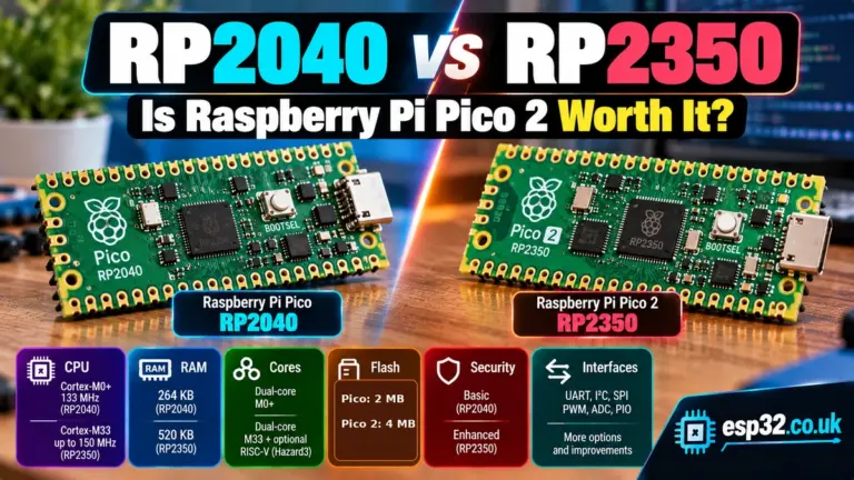
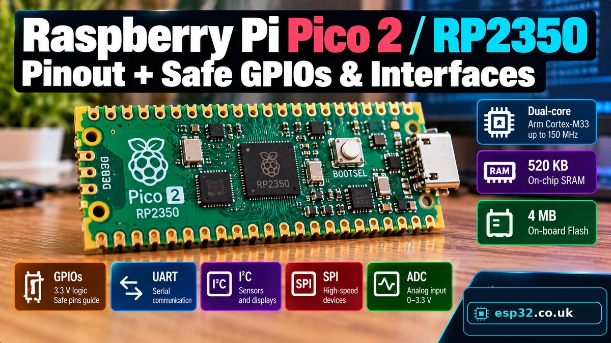
The Raspberry Pi Pico 2AliExpress price is a 21 × 51 mm microcontroller board based on the RP2350A. It provides dual 150 MHz Arm Cortex-M33 cores or dual Hazard3 RISC-V cores, 520 KB SRAM, 4 MB onboard QSPI flash, USB 1.1 device/host, two UARTs, two SPI controllers, two I²C controllers, a 12-bit 500 kS/s ADC, 12 PWM slices and three PIO blocks with 12 state machines. The board exposes 26 multi-function 3.3 V GPIOs: GPIO0–22 and GPIO26–28. GPIO26, GPIO27 and GPIO28 are the three exposed ADC inputs. Unlike ESP32AliExpress price, Pico 2AliExpress price has no exposed boot-strapping GPIOs that need to be avoided for normal startup; the board keeps GPIO23, GPIO24, GPIO25 and GPIO29 for internal SMPS, VBUS, LED and VSYS functions. The main safety rule is electrical: Pico 2AliExpress price GPIO is 3.3 V logic and is not a 5 V GPIO interface. GPIO26–28 have an additional analogue-pad restriction and should never be driven beyond the 3.3 V domain. Programming is exceptionally simple: hold BOOTSEL while connecting USB and copy a UF2 file to the mass-storage device. SWD is available for debugging.
What Is Raspberry Pi Pico 2?
Raspberry Pi Pico 2AliExpress price is the second-generation Pico microcontroller board. It looks deliberately similar to the original RP2040-based Pico so that existing breadboards, carrier boards and many accessories can continue to work, but the microcontroller underneath has changed substantially.
The board uses the RP2350A, Raspberry Pi’s second-generation microcontroller. The standard Pico 2 has no Wi-Fi or Bluetooth. If you need wireless connectivity, the Pico 2 W uses the same RP2350 generation while adding 2.4 GHz Wi-Fi and Bluetooth.
Like the original Pico, Pico 2 is a microcontroller board rather than a Linux single-board computer. It boots directly into your firmware and is programmed using MicroPython, C/C++, Arduino-compatible cores and other RP2350 toolchains.
Raspberry Pi Pico 2 Specifications
| Feature | Raspberry Pi Pico 2 |
|---|---|
| Microcontroller | RP2350A |
| CPU options | Dual Arm Cortex-M33 or dual Hazard3 RISC-V |
| Maximum clock | 150 MHz |
| SRAM | 520 KB |
| Onboard flash | 4 MB QSPI |
| Exposed GPIO | 26 multi-function 3.3 V GPIO |
| Exposed ADC inputs | 3 — GPIO26, GPIO27, GPIO28 |
| ADC | 12-bit SAR, 500 kS/s |
| UART | 2 |
| SPI | 2 |
| I²C | 2 |
| PWM | 12 slices / up to 24 controllable PWM outputs at RP2350 level |
| PIO | 3 blocks / 12 state machines |
| USB | USB 1.1 controller + PHY, device and host support |
| Programming | USB BOOTSEL mass-storage UF2 or SWD |
| Board dimensions | 21 × 51 mm |
| Input supply via VSYS | 1.8–5.5 V |
| GPIO voltage | 3.3 V fixed on Pico 2 |
| Operating temperature | −20 °C to +85 °C component limit; Raspberry Pi recommends max 70 °C ambient |
RP2350’s unusual feature is the choice of processor architecture. Firmware can target either the pair of Cortex-M33 cores or the pair of Hazard3 RISC-V cores. It is not a four-core processor running two Arm and two RISC-V cores simultaneously.
Pico 2 Pinout at a Glance
                    Micro-USB
                       │
                       ▼
          ┌─────────────────────────┐
 GP0   1  │●                       ●│ 40  VBUS
 GP1   2  │●                       ●│ 39  VSYS
 GND   3  │●                       ●│ 38  GND
 GP2   4  │●                       ●│ 37  3V3_EN
 GP3   5  │●                       ●│ 36  3V3(OUT)
 GP4   6  │●                       ●│ 35  ADC_VREF
 GP5   7  │●                       ●│ 34  GP28 / ADC2
 GND   8  │●                       ●│ 33  AGND
 GP6   9  │●                       ●│ 32  GP27 / ADC1
 GP7  10  │●       RP2350A         ●│ 31  GP26 / ADC0
 GP8  11  │●                       ●│ 30  RUN
 GP9  12  │●                       ●│ 29  GP22
 GND  13  │●                       ●│ 28  GND
 GP10 14  │●                       ●│ 27  GP21
 GP11 15  │●                       ●│ 26  GP20
 GP12 16  │●                       ●│ 25  GP19
 GP13 17  │●                       ●│ 24  GP18
 GND  18  │●                       ●│ 23  GND
 GP14 19  │●                       ●│ 22  GP17
 GP15 20  │●                       ●│ 21  GP16
          └──────────┬──────────────┘
                 SWD DEBUG
             SWCLK | GND | SWDIO
The 40 main pins are numbered physically from pin 1 at the top-left, down to pin 20, then from pin 21 at the bottom-right up to pin 40. The three SWD pads/connectors at the lower edge are separate from the 40-pin header.
Complete Pico 2 40-Pin Header
| Physical pin | Signal | Main useful functions |
|---|---|---|
| 1 | GPIO0 | UART0 TX / I²C0 SDA / SPI0 RX / PWM / PIO |
| 2 | GPIO1 | UART0 RX / I²C0 SCL / SPI0 CSn / PWM / PIO |
| 3 | GND | Ground |
| 4 | GPIO2 | I²C1 SDA / SPI0 SCK / PWM / PIO |
| 5 | GPIO3 | I²C1 SCL / SPI0 TX / PWM / PIO |
| 6 | GPIO4 | UART1 TX / I²C0 SDA / SPI0 RX / PWM / PIO |
| 7 | GPIO5 | UART1 RX / I²C0 SCL / SPI0 CSn / PWM / PIO |
| 8 | GND | Ground |
| 9 | GPIO6 | I²C1 SDA / SPI0 SCK / PWM / PIO |
| 10 | GPIO7 | I²C1 SCL / SPI0 TX / PWM / PIO |
| 11 | GPIO8 | UART1 TX / I²C0 SDA / SPI1 RX / PWM / PIO |
| 12 | GPIO9 | UART1 RX / I²C0 SCL / SPI1 CSn / PWM / PIO |
| 13 | GND | Ground |
| 14 | GPIO10 | I²C1 SDA / SPI1 SCK / PWM / PIO |
| 15 | GPIO11 | I²C1 SCL / SPI1 TX / PWM / PIO |
| 16 | GPIO12 | UART0 TX / I²C0 SDA / SPI1 RX / PWM / PIO |
| 17 | GPIO13 | UART0 RX / I²C0 SCL / SPI1 CSn / PWM / PIO |
| 18 | GND | Ground |
| 19 | GPIO14 | I²C1 SDA / SPI1 SCK / PWM / PIO |
| 20 | GPIO15 | I²C1 SCL / SPI1 TX / PWM / PIO |
| 21 | GPIO16 | SPI0 RX / I²C0 SDA / UART0 TX / PWM / PIO |
| 22 | GPIO17 | SPI0 CSn / I²C0 SCL / UART0 RX / PWM / PIO |
| 23 | GND | Ground |
| 24 | GPIO18 | SPI0 SCK / I²C1 SDA / PWM / PIO |
| 25 | GPIO19 | SPI0 TX / I²C1 SCL / PWM / PIO |
| 26 | GPIO20 | I²C0 SDA / PWM / PIO |
| 27 | GPIO21 | I²C0 SCL / PWM / PIO |
| 28 | GND | Ground |
| 29 | GPIO22 | GPIO / PWM / PIO |
| 30 | RUN | RP2350 enable/reset; pull low to reset |
| 31 | GPIO26 / ADC0 | Digital GPIO / ADC0 / I²C1 SDA |
| 32 | GPIO27 / ADC1 | Digital GPIO / ADC1 / I²C1 SCL |
| 33 | AGND | Analogue ground |
| 34 | GPIO28 / ADC2 | Digital GPIO / ADC2 |
| 35 | ADC_VREF | ADC supply/reference |
| 36 | 3V3(OUT) | Regulated 3.3 V output |
| 37 | 3V3_EN | SMPS enable; pull low to turn off 3.3 V rail |
| 38 | GND | Ground |
| 39 | VSYS | Main system input, 1.8–5.5 V |
| 40 | VBUS | USB 5 V input rail |
Which Pico 2 GPIOs Are Safe to Use?
This question has a simpler answer than on many ESP32 boards. The Pico 2 does not expose a set of boot-strapping GPIOs that must sit at particular logic levels during startup. The 26 GPIOs on the main header are intended for user I/O.
| GPIO group | Recommendation | Reason |
|---|---|---|
| GPIO0–22 | Safe general-purpose GPIO | All are exposed user GPIO; no board boot strapping on these header pins |
| GPIO26–28 | Safe GPIO with ADC precautions | Digital or ADC use; keep voltage inside 3.3 V analogue limits |
| GPIO23 | Do not treat as user GPIO | Internal: controls SMPS power-save mode; only available as test point |
| GPIO24 | Internal | VBUS sense |
| GPIO25 | Internal / LED | Drives onboard LED; not on main header |
| GPIO29 | Internal | ADC3 used to monitor VSYS/3 |
| SWDIO / SWCLK | Reserve for debugging | Separate debug interface, not part of the 26 main GPIO header pins |
So, for a normal project, GPIO0–22 are the easiest pins to allocate freely. GPIO26–28 are equally usable as digital GPIO, but if you might need analogue measurements later it is sensible to reserve them for ADC.
Pico 2 Is 3.3 V Logic — Do Not Feed GPIO 5 V
Pico 2’s GPIO rail is fixed at 3.3 V. The fact that the board itself can be powered from USB 5 V or from up to 5.5 V on VSYS does not make the GPIO pins 5 V-compatible.
- Do not connect a 5 V push-pull output directly to a Pico 2 GPIO.
- Use a resistor divider or level shifter for 5 V sensor/logic outputs where appropriate.
- Use 3.3 V pull-ups on I²C when devices connect directly to the RP2350.
- Do not drive motors, relays or other high-current loads directly from GPIO; use a transistor, MOSFET, driver or H-bridge.
- GPIO outputs are logic signals, not power outputs.
- If a peripheral can run at both 3.3 V and 5 V, powering its logic side at 3.3 V usually makes interfacing simpler.
Special ADC Warning for GPIO26–GPIO28
GPIO26, GPIO27 and GPIO28 are connected to RP2350’s ADC-capable pads. Raspberry Pi specifically notes that the ADC-capable GPIO26–29 group has an internal reverse diode to the I/O supply rail.
The practical rule is simple: do not let the voltage on GPIO26–28 exceed the 3.3 V I/O rail by more than the small diode margin. Treat 0–3.3 V as the normal working range.
There is another subtle difference: if RP2350 is unpowered while voltage is applied to an ADC-capable GPIO, current can leak through that diode into the 3.3 V rail. Avoid externally driving GPIO26–28 while the Pico 2 is powered off.
The ordinary digital GPIO0–22 do not have that same ADC-pad diode restriction, but they are still 3.3 V logic pins and should not be treated as 5 V inputs.
RP2350 E9 GPIO Erratum: What Pico 2 Owners Should Know
Early RP2350 silicon, the original A2 stepping, has a documented GPIO pad issue known as Erratum E9. Under affected input conditions, a pin that has been driven high can exhibit unwanted leakage instead of returning cleanly to a high-impedance/weakly pulled-low state.
This is most relevant to circuits that rely on floating inputs, very weak pull-down resistors, open-drain behaviour or high-impedance input switching. A conventional actively driven push-pull digital signal is less likely to expose the problem.
Raspberry Pi announced the A4 stepping in 2025 and states that A4 fixes E9 by correcting the GPIO pad design. If you are designing a production board or a circuit where weak pull-down/high-impedance behaviour is critical, identify the silicon revision rather than assuming every RP2350 in circulation behaves identically.
- For ordinary buttons, sensors and actively driven logic, follow the normal SDK/library recommendations.
- For an A2-based design that depends on weak pull-downs or truly high-impedance inputs, read the current RP2350 E9 erratum.
- For a new commercial design where E9 matters, prefer confirmed A4 or later silicon.
- Do not confuse E9 with a reason to avoid specific Pico 2 header GPIO numbers — it is a silicon-pad behaviour issue, not an ESP32-style list of ‘bad boot pins’.
ADC Pins and Analogue Measurements
| Physical pin | GPIO | ADC channel |
|---|---|---|
| 31 | GPIO26 | ADC0 |
| 32 | GPIO27 | ADC1 |
| 34 | GPIO28 | ADC2 |
| Internal | GPIO29 | ADC3 — measures VSYS/3 |
| Internal | Temperature sensor | Internal ADC mux input |
RP2350’s ADC is a 12-bit SAR converter running at up to 500 kS/s. The Pico 2 exposes three external analogue inputs; the fourth RP2350A ADC-capable GPIO, GPIO29, is used internally to measure the system supply through a divide-by-three network.
Pico 2 provides separate ADC_VREF and AGND pins to make cleaner analogue designs possible. The standard ADC reference is derived from the board’s 3.3 V supply through filtering, so absolute measurement accuracy is limited by supply accuracy, noise and ADC offset.
For precision measurement, Raspberry Pi documents the option of using a suitable external shunt reference on ADC_VREF. For ordinary potentiometers, light sensors and analogue sensors, the standard arrangement is normally sufficient.
MicroPython ADC Example
from machine import ADC
from time import sleep

adc = ADC(26)   # GPIO26 / ADC0

while True:
    raw = adc.read_u16()
    voltage = raw * 3.3 / 65535
    print(raw, voltage)
    sleep(0.5)
MicroPython presents ADC readings using its standard API scaling, so the returned numerical width is an API representation rather than a claim that the RP2350 ADC hardware is 16-bit. The hardware converter is 12-bit.
I²C Pin Options
RP2350 has two hardware I²C controllers, and the GPIO matrix exposes each controller on multiple pin pairs. That means you are not locked to one SDA/SCL pair.
| I²C bus | Convenient SDA pins | Convenient SCL pins |
|---|---|---|
| I²C0 | GPIO0, GPIO4, GPIO8, GPIO12, GPIO16, GPIO20 | GPIO1, GPIO5, GPIO9, GPIO13, GPIO17, GPIO21 |
| I²C1 | GPIO2, GPIO6, GPIO10, GPIO14, GPIO18, GPIO26 | GPIO3, GPIO7, GPIO11, GPIO15, GPIO19, GPIO27 |
Choose the pair that best fits your physical wiring and other peripheral assignments. SDA and SCL need to come from the same I²C controller and a valid matching mapping.
from machine import I2C, Pin

i2c = I2C(
    0,
    scl=Pin(1),
    sda=Pin(0),
    freq=400000
)

print(i2c.scan())
I²C requires pull-up resistors. Many breakout boards already include them; make sure any pull-ups connected directly to Pico 2 go to 3.3 V rather than 5 V.
SPI Pin Options
Pico 2 includes two hardware SPI controllers. The official pinout highlights several convenient mappings.
| Example SPI bus | RX / MISO | CSn | SCK | TX / MOSI |
|---|---|---|---|---|
| SPI0 option A | GPIO0 | GPIO1 | GPIO2 | GPIO3 |
| SPI0 option B | GPIO4 | GPIO5 | GPIO6 | GPIO7 |
| SPI0 option C | GPIO16 | GPIO17 | GPIO18 | GPIO19 |
| SPI1 option A | GPIO8 | GPIO9 | GPIO10 | GPIO11 |
| SPI1 option B | GPIO12 | GPIO13 | GPIO14 | GPIO15 |
Chip-select is often controlled as an ordinary GPIO in software, so practical SPI wiring can be even more flexible than the table suggests. Keep fast SPI traces short and provide a solid ground reference.
from machine import SPI, Pin

spi = SPI(
    0,
    baudrate=10_000_000,
    polarity=0,
    phase=0,
    sck=Pin(18),
    mosi=Pin(19),
    miso=Pin(16)
)

cs = Pin(17, Pin.OUT, value=1)
UART Pin Options
RP2350 provides two UART controllers. As with I²C and SPI, UART functions appear on several GPIO pairs.
| UART | TX examples | RX examples |
|---|---|---|
| UART0 | GPIO0, GPIO12, GPIO16 | GPIO1, GPIO13, GPIO17 |
| UART1 | GPIO4, GPIO8 | GPIO5, GPIO9 |
from machine import UART, Pin

uart = UART(
    0,
    baudrate=115200,
    tx=Pin(0),
    rx=Pin(1)
)

uart.write("Pico 2 UART ready\r\n")
The USB port can also provide a serial console through firmware, so hardware UART pins can remain available for GPS modules, motor controllers, industrial interfaces or other peripherals.
PWM on Pico 2
RP2350 expands the PWM subsystem to 12 slices, each with two channels. At the microcontroller level that provides up to 24 controllable PWM outputs, subject to GPIO mapping and shared slice-frequency constraints.
PWM is useful for LED dimming, servo control, motor-driver commands, switching regulators, audio experiments and pulse/frequency generation. It is not a true analogue voltage output; the pin still switches between logic low and high.
from machine import Pin, PWM
from time import sleep

pwm = PWM(Pin(15))
pwm.freq(1000)

while True:
    for duty in range(0, 65535, 1024):
        pwm.duty_u16(duty)
        sleep(0.01)
PIO: Pico 2’s Most Flexible Interface
Programmable I/O is one of the defining features of Raspberry Pi microcontrollers. Instead of relying only on fixed UART, SPI or I²C blocks, PIO uses small deterministic state machines that can generate or sample digital waveforms with precise timing.
RP2350 increases the count from two PIO blocks on RP2040 to three PIO blocks with 12 state machines total. PIO can implement protocols and timing engines that would otherwise require a dedicated peripheral, CPLD or carefully timed CPU code.
- WS2812 / NeoPixel LED output
- Custom serial protocols
- VGA-style signalling
- I²S and digital audio
- Additional UART/SPI-style interfaces
- Precise pulse generation and capture
- Quadrature and protocol decoding
- SD-card-style interfaces and other high-speed digital tasks
PIO is one reason the answer to ‘which pin can do this?’ is often ‘almost any sensible digital GPIO’ on Pico 2. PIO includes flexible internal pin mapping rather than requiring one fixed peripheral location.
USB: Device, Host and BOOTSEL
RP2350 includes a USB 1.1 controller and PHY with both device and host support. Pico 2 connects it to the Micro-USB socket.
In normal firmware, USB can provide CDC serial, HID, MIDI and other supported classes. In host mode the Pico 2 can communicate with USB devices, but host-mode power requires more care: Raspberry Pi specifies that Pico 2 must be provided with 5 V on VBUS for USB-host operation.
BOOTSEL Programming
- Disconnect/depower the Pico 2.
- Hold the BOOTSEL button.
- Connect USB while continuing to hold BOOTSEL.
- Release the button after the board enumerates.
- A USB mass-storage device appears on the computer.
- Copy the appropriate .uf2 firmware file to the drive.
- Pico 2 writes the flash and reboots into the new firmware.
The USB boot code lives in RP2350 mask ROM, so a broken application cannot erase it. That makes Pico 2 unusually easy to recover compared with microcontroller boards that depend on a flash-resident bootloader.
BOOTSEL Is Not a GPIO-Strapping Problem
BOOTSEL is sometimes mistaken for an ESP32-style boot strap attached to one of the exposed GPIO pins. It is not. On the Pico 2 board, BOOTSEL is handled as a dedicated boot mechanism and does not require you to keep GPIO0, GPIO2 or another header GPIO at a particular state during normal startup.
That is why the Pico 2 ‘safe GPIO’ list is refreshingly simple: allocate GPIO0–22 as your project requires, reserve GPIO26–28 when you need ADC, and obey the voltage/electrical rules.
SWD Debugging
| Debug signal | Pico 2 debug connector |
|---|---|
| SWCLK | SWCLK |
| GND | GND |
| SWDIO | SWDIO |
Serial Wire Debug lets a debugger/programmer reset the RP2350, load firmware and inspect a running program. The original headerless Pico 2 exposes three debug pads/holes at the lower edge; some header-equipped versions use a small keyed debug connector.
A Raspberry Pi Debug Probe or another compatible SWD debugger is useful when projects become too complex for print statements and USB serial debugging.
Power Pins Explained
| Pin | Meaning | Practical use |
|---|---|---|
| VBUS — pin 40 | USB input voltage, nominal 5 V | USB power rail; not a GPIO supply level |
| VSYS — pin 39 | 1.8–5.5 V main system input | Battery/external supply input to board SMPS |
| 3V3(OUT) — pin 36 | Regulated 3.3 V output | Power 3.3 V sensors and logic; Raspberry Pi recommends external load under 300 mA |
| 3V3_EN — pin 37 | SMPS enable | Pull low to turn off 3.3 V rail and RP2350 |
| ADC_VREF — pin 35 | ADC reference/supply | Analogue reference; can be externally conditioned for precision |
| AGND — pin 33 | Analogue ground | Preferred return for analogue sensor circuitry |
| RUN — pin 30 | RP2350 enable/reset | Short low to reset the MCU |
Pico 2 uses a buck-boost SMPS, which is why VSYS can operate across such a wide 1.8–5.5 V input range. That makes single-cell battery and multi-cell AA applications straightforward.
The board’s USB-to-VSYS path includes a Schottky diode. Raspberry Pi documents diode-OR and P-channel MOSFET arrangements for safely combining USB with an external power source instead of simply tying independent supplies together.
Onboard LED
On the non-wireless Pico 2, the onboard LED is connected internally to GPIO25. GPIO25 is not one of the 26 GPIO pins exposed on the main 40-pin header.
from machine import Pin
from time import sleep

led = Pin("LED", Pin.OUT)

while True:
    led.toggle()
    sleep(0.5)
Using the symbolic LED name is preferable when you want code that can also run on wireless Pico variants, because the LED implementation differs on W models.
MicroPython Setup
- Download the current MicroPython UF2 for Raspberry Pi Pico 2 from Raspberry Pi/MicroPython.
- Hold BOOTSEL while connecting Pico 2 by USB.
- Copy the UF2 file to the mass-storage drive.
- Open Thonny or another MicroPython editor/serial REPL.
- Select the Pico 2 MicroPython interpreter/serial device.
- Test with the onboard LED example.
MicroPython is the fastest route to a working Pico 2 project and is excellent for sensors, I²C displays, prototypes and teaching. C/C++ is a better fit when deterministic timing, maximum performance or direct SDK features matter.
Arduino IDE on Pico 2
Pico 2 can also be used from Arduino IDE through the widely used community Arduino-Pico core by Earle F. Philhower. The core supports both RP2040 and RP2350, including the Raspberry Pi Pico 2 target.
Add the following Boards Manager URL in Arduino IDE’s Additional Boards Manager URLs:
https://github.com/earlephilhower/arduino-pico/releases/download/global/package_rp2040_index.json- Open Boards Manager and install the Raspberry Pi Pico/RP2040/RP2350 Arduino package.
- Select Raspberry Pi Pico 2.
- For the first upload, use BOOTSEL while connecting the board if required.
- After a successful Arduino-Pico upload, normal auto-reset uploading is usually available while the firmware/USB connection remains responsive.
const int led = LED_BUILTIN;

void setup() {
  pinMode(led, OUTPUT);
}

void loop() {
  digitalWrite(led, HIGH);
  delay(500);
  digitalWrite(led, LOW);
  delay(500);
}
Pico 2 vs Pico 2 W Pinout
Pico 2 W keeps the same broad 40-pin compatibility concept, but the wireless board has internal differences because the radio subsystem and onboard LED are connected through the wireless hardware. Do not assume every internal GPIO detail from the non-wireless Pico 2 also applies to Pico 2 W.
For ordinary external GPIO, I²C, SPI, UART, ADC and power wiring, the Pico 2 W is deliberately designed to preserve Pico-family compatibility. For radio-specific or onboard-LED behaviour, use the Pico 2 W documentation.
Pico 2 vs Original Pico: Pin Compatibility
One of Raspberry Pi’s design goals was hardware and software compatibility with the original Pico. The non-wireless Pico 2 maintains the same 40-pin header layout, which makes it unusually easy to upgrade an existing RP2040 project.
| Feature | Original Pico / RP2040 | Pico 2 / RP2350 |
|---|---|---|
| Header format | 40-pin Pico layout | Same layout |
| Exposed GPIO | 26 | 26 |
| External ADC pins | 3 | 3 |
| CPU | Dual Cortex-M0+ @ 133 MHz | Dual Cortex-M33 or Hazard3 @ 150 MHz |
| SRAM | 264 KB | 520 KB |
| Onboard flash | 2 MB | 4 MB |
| PIO | 2 blocks / 8 state machines | 3 blocks / 12 state machines |
| USB | USB 1.1 device/host | USB 1.1 device/host |
| Security | Basic | TrustZone, secure boot features, OTP, SHA-256, TRNG |
Recommended Pin Allocation for a Typical Project
Raspberry Pi Pico 2
├─ I2C sensors
│  ├─ GPIO0  SDA
│  └─ GPIO1  SCL
├─ SPI display / SD / peripheral
│  ├─ GPIO18 SCK
│  ├─ GPIO19 MOSI
│  ├─ GPIO16 MISO
│  └─ GPIO17 CS
├─ UART device
│  ├─ GPIO4 TX
│  └─ GPIO5 RX
├─ Analogue sensors
│  ├─ GPIO26 ADC0
│  ├─ GPIO27 ADC1
│  └─ GPIO28 ADC2
├─ General digital I/O
│  └─ GPIO2–15, GPIO20–22 as required
├─ Debug
│  └─ Separate SWD header
└─ Power
   ├─ 3V3(OUT) for 3.3 V sensors
   ├─ GND / AGND
   └─ VSYS for external board power
This is only one clean allocation. Pico 2’s peripheral multiplexing and PIO mean there are many equally valid layouts. The best pinout is the one that avoids physical crossing, preserves ADC pins if needed and keeps fast digital signals short and well-grounded.
Common Pico 2 Wiring Mistakes
| Mistake | Why it causes problems | Better approach |
|---|---|---|
| Feeding a GPIO with 5 V | Pico 2 I/O is fixed at 3.3 V | Level-shift or divide the signal |
| Driving GPIO26–28 while Pico 2 is off | ADC pads can leak into IOVDD rail | Remove the external drive or provide proper isolation |
| Confusing VSYS with a 3.3 V pin | VSYS is the SMPS input and can be up to 5.5 V | Use 3V3(OUT) for 3.3 V peripherals |
| Using VBUS as logic power | VBUS is nominal USB 5 V | Use 3V3(OUT) unless the peripheral explicitly needs 5 V |
| No I²C pull-ups | Open-drain bus needs pull-ups | Use appropriate pull-ups to 3.3 V |
| Powering a motor directly from GPIO | GPIO cannot supply motor current or absorb inductive transients | Use driver/MOSFET/H-bridge and protection |
| Assuming ADC is precision 12-bit instrumentation | Reference/supply noise and offset matter | Calibrate, average or use external reference/ADC |
| Treating E9 as a list of bad GPIO numbers | E9 is an early-silicon pad behaviour issue | Read E9 if weak pull-down/high-Z behaviour matters; A4 fixes it |
| Losing a broken firmware upload path | Application USB can crash | BOOTSEL ROM USB mode remains recoverable |
Who Should Choose Pico 2?
- You want a low-cost microcontroller with significantly more RAM than classic Arduino-class boards.
- You need deterministic GPIO and programmable PIO rather than built-in wireless.
- You want to learn Arm Cortex-M33 or experiment with RISC-V on the same RP2350 platform.
- You need USB device or USB host support.
- You are upgrading an existing original Pico design and want strong pin compatibility.
- You want MicroPython for fast prototyping but also a serious C/C++ SDK when the project grows.
- You need flexible battery input through the board’s 1.8–5.5 V VSYS power architecture.
When ESP32 Is the Better Choice
Pico 2 is a powerful microcontroller, but it does not have built-in Wi-Fi or Bluetooth. If the project is primarily about MQTT, ESPHome, Home Assistant, BLE or Wi-Fi connectivity, an ESP32 is normally the simpler choice.
If you like the RP2350 platform but need wireless, use Pico 2 W. If you need ESPHome’s mature device ecosystem and deep Home Assistant integration, ESP32 remains the natural fit.
For precise custom digital interfaces, PIO-heavy designs, USB devices or projects where you want to explore both Arm and RISC-V, Pico 2 has a very different and compelling set of strengths.
Final Recommendation
Raspberry Pi Pico 2 is one of the easiest modern microcontroller boards to allocate pins on because Raspberry Pi has kept the special board functions away from the main user GPIO header. You get 26 genuinely useful 3.3 V GPIOs, with GPIO26–28 adding ADC capability.
The essential safety rules are simple: do not feed 5 V into GPIO, pay extra attention to the ADC-pad restrictions on GPIO26–28, use the correct VBUS/VSYS/3V3 power pin, and use external drivers for loads that require real current.
For early A2 RP2350 silicon, also understand E9 if your circuit depends on high-impedance inputs or weak pull-downs. The later A4 stepping fixes that pad issue. For normal development, BOOTSEL gives you an almost impossible-to-brick USB recovery path, while SWD is available when you need real debugging.
Related Guides
- RP2040 vs RP2350: Raspberry Pi Pico vs Pico 2 Compared
- Raspberry Pi Pico W vs ESP32: Which Is Better for IoT & Home Assistant?
- ESP32 DevKitC V4 Pinout Diagram & Safe GPIOs
- ESP32-S3 DevKitC-1 Pinout Diagram & Safe GPIOs
Datasheets & External Resources
- Raspberry Pi Pico 2 Datasheet — official 2026 board pinout, GPIO, ADC, power, USB and SWD documentation.
- RP2350 Datasheet — complete RP2350 peripheral, electrical and errata reference.
- Raspberry Pi Pico-Series Documentation — board variants, pin functions and getting-started resources.
- Pico SDK Hardware APIs — current ADC, GPIO, PWM and peripheral APIs.
- RP2350 A4 Announcement — Raspberry Pi explanation of A4 silicon and the E9 GPIO fix.
- Raspberry Pi Pico 2 Product Page — official board overview and specifications.
- Arduino-Pico — community Arduino core supporting RP2040 and RP2350/Pico 2.