
The PCF8591 YL-40 ADC/DAC module adds four 8-bit analogue input channels and one 8-bit analogue voltage output to an ESP32AliExpress price using only I²C SDA and SCL. Unlike a simple bare-chip breakout, the widely sold YL-40 board also carries a light-dependent resistor (LDR), a thermistorAliExpress price and a blue adjustable potentiometer. Three removable jumper caps choose whether those onboard circuits feed the ADC channels. This reference explains the board silkscreen, safe 3.3 V wiring, fixed-versus-programmable addresses, the I²C read protocol and a complete Arduino IDE example using the built-in Wire library.
Quick answer: A typical YL-40 is found at 0x48; AIN0 reads the light sensorAliExpress price, AIN1 the thermistor, AIN3 the trimpot, and AIN2 is normally free for an external voltage. Remove a sensor jumper before using its channel for an unrelated analogue signal. The PCF8591 is only 8-bit; it is a useful teaching and control module, not a high-precision voltmeter.
What does the PCF8591 module do?
| Feature | PCF8591 / common YL-40 module |
|---|---|
| ADC inputs | Four multiplexed 8-bit channels: AIN0–AIN3 |
| DAC output | One 8-bit output, AOUT; 256 nominal digital settings |
| Interface | I²C, SDA and SCL; use 7-bit address in Arduino Wire |
| Chip supply | 2.5–6.0 V according to the original NXP datasheet |
| ESP32 connection | Use 3.3 V supply so I²C pull-ups cannot reach 5 V |
| Reference | VREF and AGND set the analogue conversion span; typically tied to board supply and ground |
| Input modes | Four single-ended inputs, or supported differential combinations |
| Selectable addresses | Chip: 0x48–0x4F by A0–A2; typical YL-40 board: fixed 0x48 |
| Onboard circuits | LDR, NTC thermistor, trimmer potentiometer; power and DAC indicator LEDs on many boards |
The original NXP PCF8591 product page now marks this IC as end of life. Existing boards still appear in educational kits and retail listings. For a new production design, check supply availability and consider a current ADC or DAC instead. The device remains worthwhile as an introduction to I²C analogue conversion.
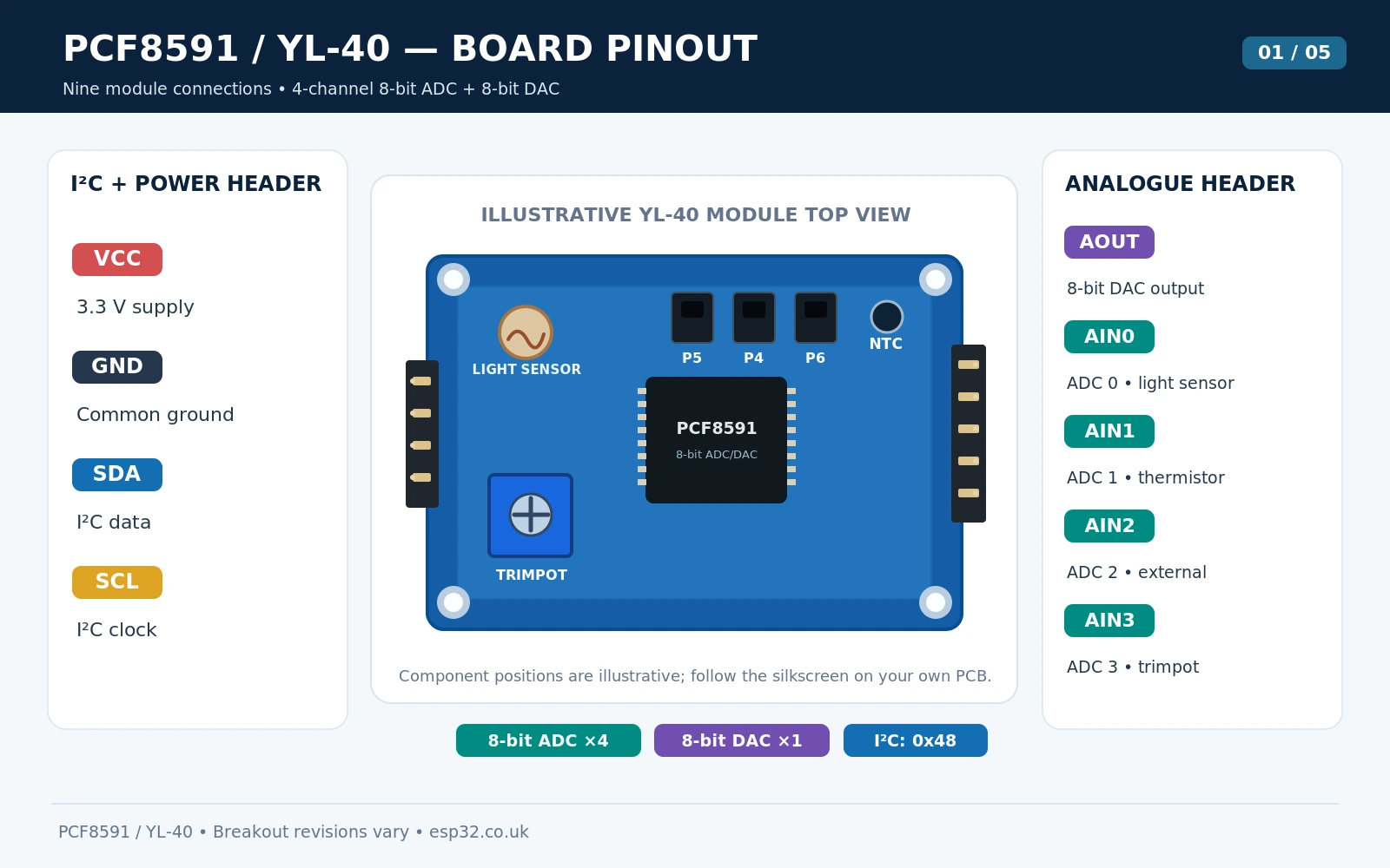
YL-40 board pinout: every connection explained
| Marking | Direction / meaning | ESP32 or external connection |
|---|---|---|
| VCC | Board supply | ESP32 3V3 (recommended for direct I²C) |
| GND | Common ground | ESP32 GND and external-signal ground |
| SDA | I²C data, bidirectional | ESP32 GPIO21 on a classic ESP32 DevKit example |
| SCL | I²C clock | ESP32 GPIO22 on the same example |
| AIN0 | 8-bit ADC channel 0 | Onboard LDR if fitted jumper; otherwise external input |
| AIN1 | 8-bit ADC channel 1 | Onboard thermistor if fitted jumper; otherwise external input |
| AIN2 | 8-bit ADC channel 2 | Usually available for an external voltage |
| AIN3 | 8-bit ADC channel 3 | Onboard potentiometer if fitted jumper; otherwise external input |
| AOUT | 8-bit DAC analogue output | External high-impedance load or meter; output LED may load it |
Common boards group VCC, GND, SDA, SCL on one four-pin header and AOUT, AIN0, AIN1, AIN2, AIN3 on another. Do not infer the left-to-right position from a photograph rotated 180 degrees: follow the actual silk-screen text beside your own header. These board signals are not the 16 physical pins of the bare PCF8591 IC; for the IC pin numbers consult the NXP DIP16/SO16 pin diagram.
A typical YL-40 has no regulator or 5 V to 3.3 V bidirectional level shifter. A chip rated for 5 V does not make a module powered from 5 V directly compatible with an ESP32. A module’s SDA/SCL pull-ups often go to its VCC. Feeding the YL-40 from 3.3 V keeps those pull-ups in the ESP32 logic range.
What do the three PCF8591 jumpers do?
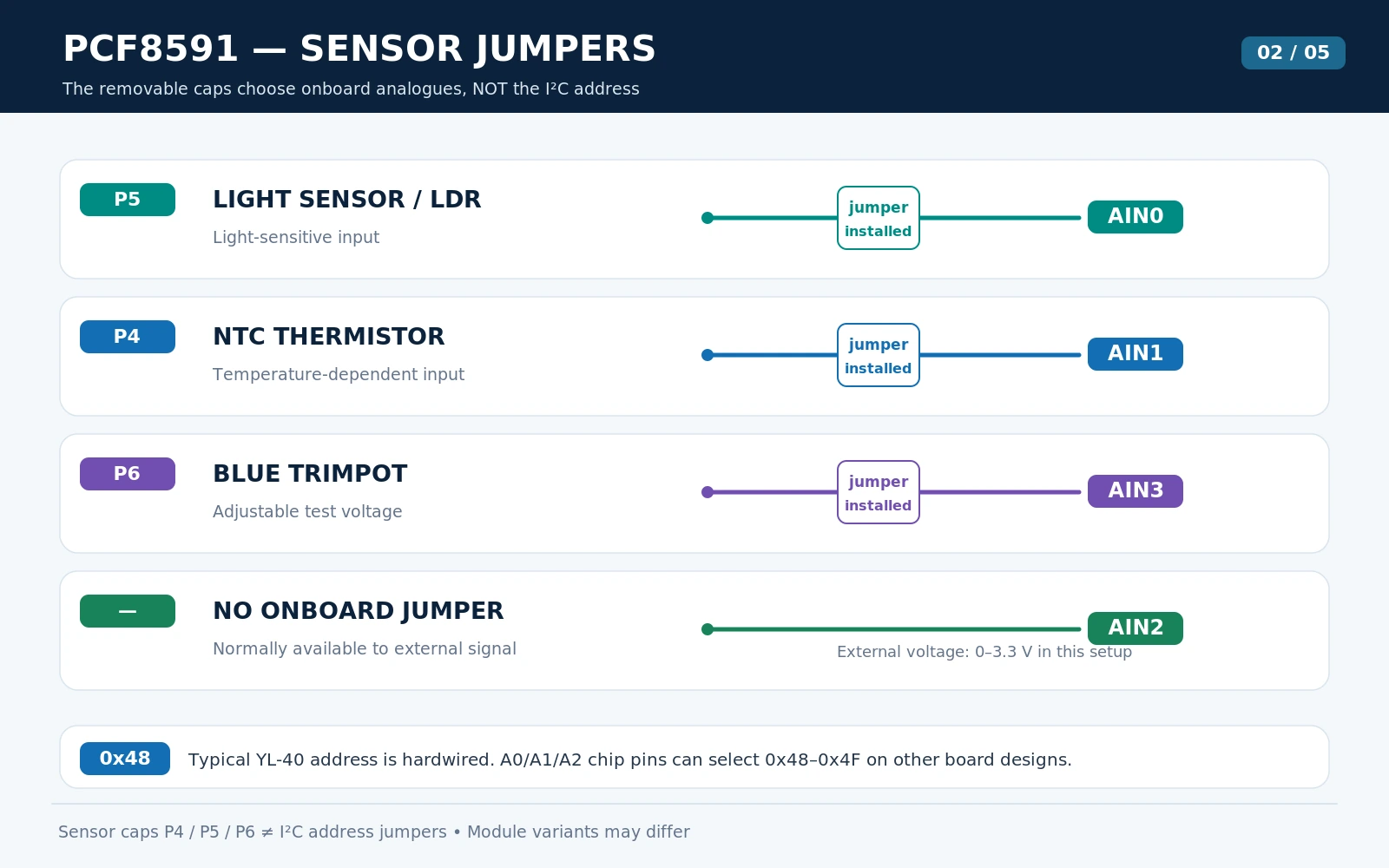
This is the detail most brief PCF8591 tutorials miss. The three jumper caps do not select the I²C address. They connect individual onboard analogue sources to individual converter inputs. With the jumper removed, that ADC header pin can accept an external signal, subject to the board’s reference and supply limits.
| Typical YL-40 marking | Onboard circuit | ADC input | With jumper removed |
|---|---|---|---|
| P5 (sometimes J5) | Photoresistor / LDR | AIN0 | AIN0 available for an external input |
| P4 (sometimes J4) | NTC thermistor | AIN1 | AIN1 available for an external input |
| P6 (sometimes J6) | Adjustable trimpot | AIN3 | AIN3 available for an external input |
| No sensor jumper | No default onboard circuit | AIN2 | AIN2 normally available already |
Board-revision warning: P4/P5/P6 and J4/J5/J6 are labels found on particular YL-40 versions, not a universal mechanical layout. Other manufacturers use alternative jumper positions or wire the sensors to different analogue channels. Identify the printed channel and trace or measure the jumper if your PCB differs.
Does soldering a pad change the I²C address?
On the PCF8591 chip, three hardware address inputs A0, A1 and A2 determine the 7-bit address:
| A2 | A1 | A0 | 7-bit I²C address |
|---|---|---|---|
| 0 | 0 | 0 | 0x48 |
| 0 | 0 | 1 | 0x49 |
| 0 | 1 | 0 | 0x4A |
| 0 | 1 | 1 | 0x4B |
| 1 | 0 | 0 | 0x4C |
| 1 | 0 | 1 | 0x4D |
| 1 | 1 | 0 | 0x4E |
| 1 | 1 | 1 | 0x4F |
However, the usual YL-40 PCB ties all three address inputs low and provides no user-selectable A0/A1/A2 solder pads. It therefore remains at 0x48, even when you remove its P4/P5/P6 caps. Changing the address is possible only on board designs exposing these address pins, or by an accurately verified PCB modification. Never randomly bridge an unlabelled pad to experiment.
Some datasheets express the write address as the 8-bit value 0x90 (and read as 0x91). Arduino Wire uses the 7-bit address 0x48 instead. Do not pass 0x90 to Wire.beginTransmission().
PCF8591 functional schematic: chip versus breakout
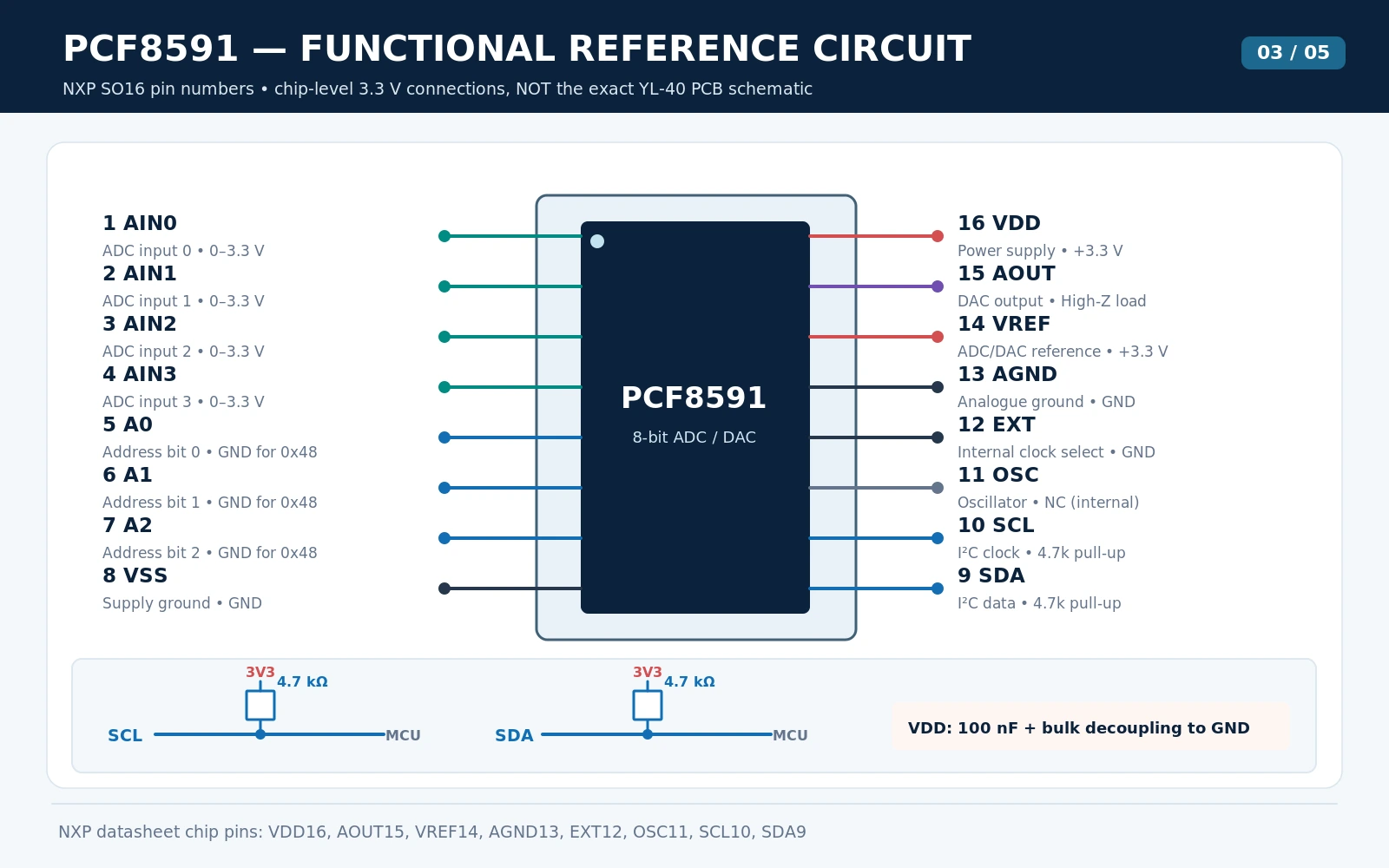
The PCF8591 contains an analogue multiplexer feeding an 8-bit successive-approximation ADC, and a separate control path to the 8-bit DAC output. A standard minimal circuit needs its supply, common ground, reference, I²C bus, and oscillator configuration. On many modules VREF is tied to VCC, AGND to ground and EXT selects the internal oscillator. Verify those nets against the actual board schematic when precision matters.
For a 3.3 V supply and a 3.3 V reference, nominal ADC resolution is 3.3 V / 256 ≈ 12.9 mV per code. That is the nominal code width, not guaranteed measurement accuracy. Any reference variation, sensor-divider nonlinearity, offset, noise and module component tolerances affect the result.
The DAC uses the reference and provides an analogue voltage at AOUT. Many YL-40 boards attach an indicator LED circuit to this output, so the observed maximum voltage can fall below the ideal unloaded value. Do not assume the DAC can drive a relay, motor or other heavy load directly.
ESP32-to-PCF8591 wiring: four I²C connections
| ESP32 DevKit (classic ESP32) | PCF8591 YL-40 | Purpose |
|---|---|---|
| 3V3 | VCC | 3.3 V board supply |
| GND | GND | Common reference |
| GPIO21 | SDA | I²C data |
| GPIO22 | SCL | I²C clock |
These GPIO numbers are an example for common ESP32-WROOM development boards, not a promise about every ESP32-C3, S3, C6, P4 or other board. If you already have an I²C bus, connect to its chosen SDA/SCL pins and initialise Wire.begin(SDA, SCL) accordingly. Check whether the YL-40 has onboard pull-ups before adding more; too many parallel pull-ups can load the bus.
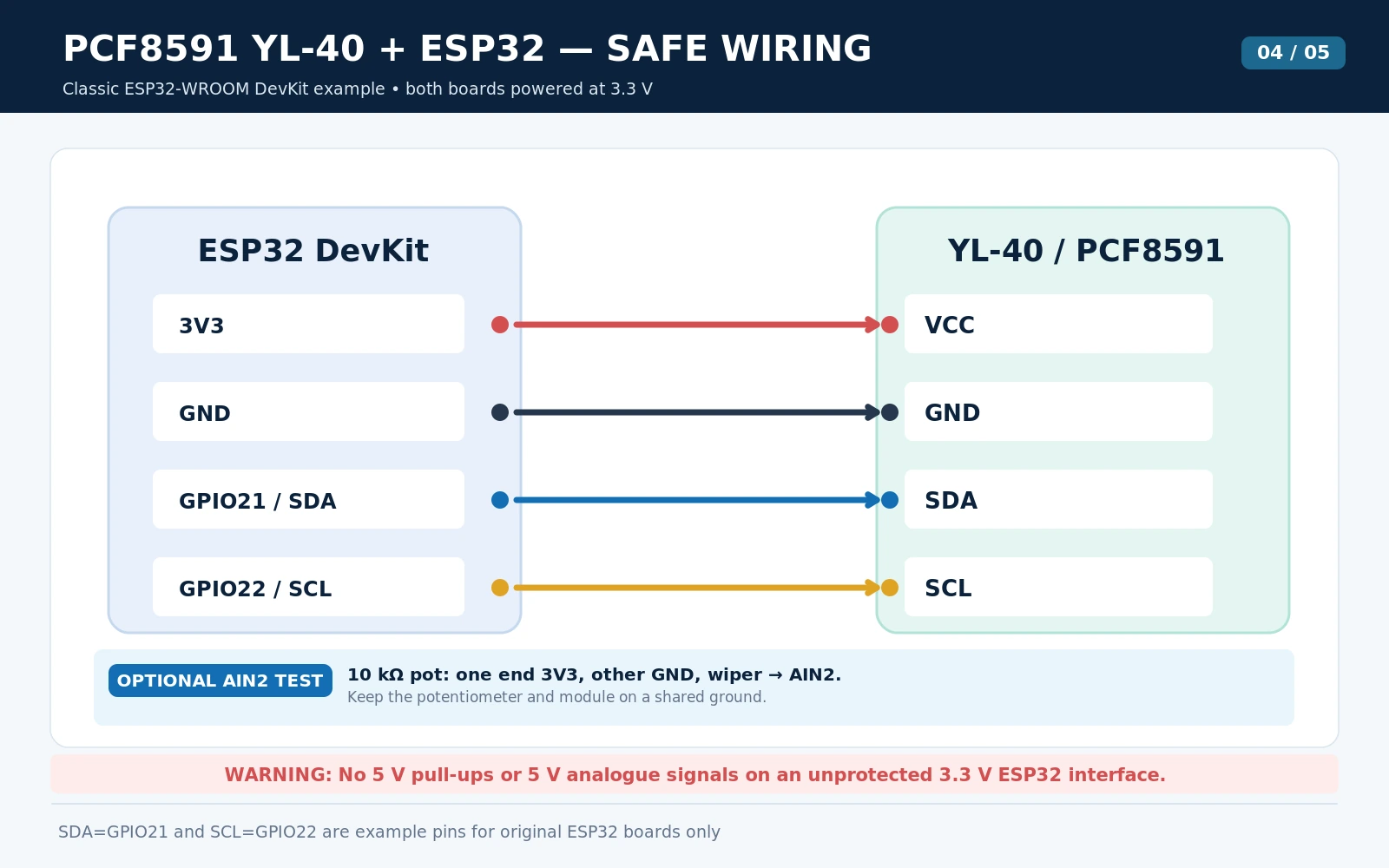
To test an independent external signal, connect a 10 kΩ potentiometer between 3V3 and GND and connect its wiper to AIN2. Its wiper voltage will sweep safely through approximately 0–3.3 V. Do not attach a 5 V sensor output to an input while the module is powered at 3.3 V. Keep all input voltages within the permitted supply/reference range and ensure grounds are shared.
Arduino IDE example: read all four channels and output a DAC ramp
For this chip, the standard Arduino Wire library is a strong choice: the protocol is tiny, transparent, and it avoids depending on an unmaintained PCF8591 wrapper. Install the ESP32 boards package through Boards Manager; Wire.h is already supplied. Select your ESP32 board, paste the following complete sketch and open Serial Monitor at 115200 baud.
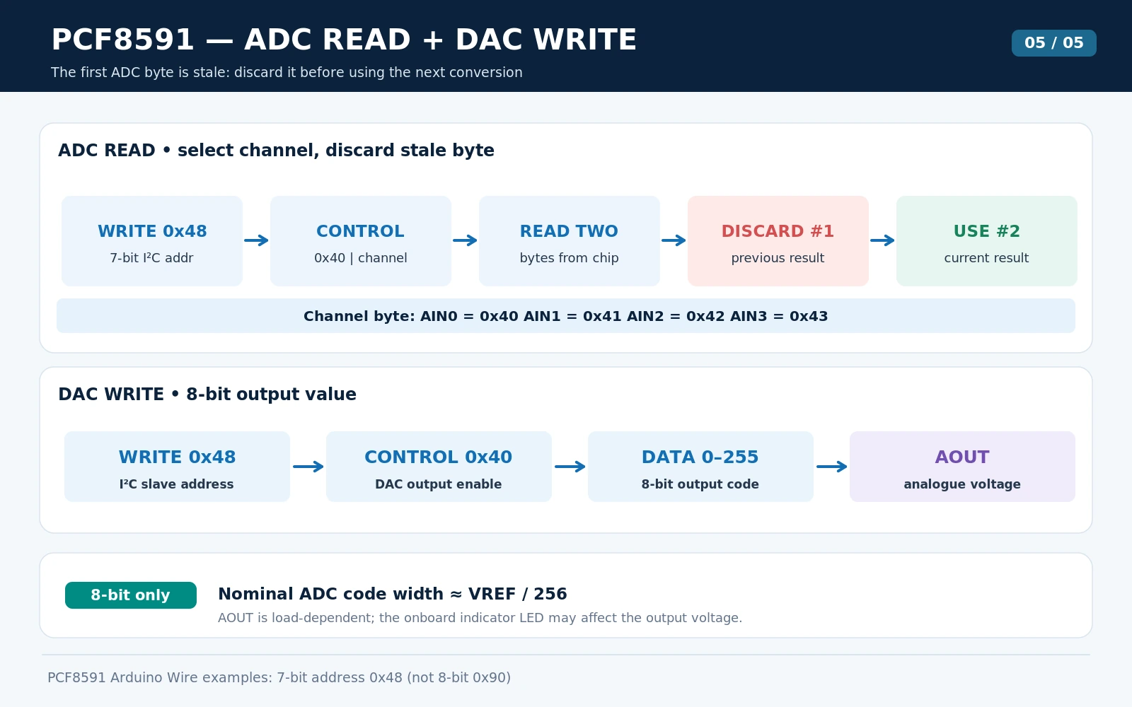
The subtlety is that a PCF8591 read returns the previous conversion result first. The function below requests two bytes after choosing a channel, discards the stale first byte, and uses the second byte as the new channel value. Keeping bit 6 set (0x40) also leaves the DAC output enabled while reading.
#include <Arduino.h>
#include <Wire.h>

constexpr uint8_t PCF_ADDR = 0x48;
constexpr int SDA_PIN = 21;
constexpr int SCL_PIN = 22;

bool writeDac(uint8_t outputValue) {
  Wire.beginTransmission(PCF_ADDR);
  Wire.write(0x40);          // DAC enabled, single-ended ADC mode
  Wire.write(outputValue);   // DAC data: 0..255
  return Wire.endTransmission() == 0;
}

// Read one PCF8591 single-ended ADC input.
// The first received byte belongs to the previous conversion.
bool readAdc(uint8_t channel, uint8_t &value) {
  if (channel > 3) return false;

  Wire.beginTransmission(PCF_ADDR);
  Wire.write(uint8_t(0x40 | channel)); // DAC stays enabled
  if (Wire.endTransmission() != 0) return false;

  if (Wire.requestFrom(PCF_ADDR, uint8_t(2)) != 2) {
    return false;
  }

  (void)Wire.read();    // Discard old conversion
  value = Wire.read();  // Current channel conversion
  return true;
}

void setup() {
  Serial.begin(115200);
  delay(500);
  Wire.begin(SDA_PIN, SCL_PIN);
  Wire.setClock(100000);  // Standard-mode I2C

  Wire.beginTransmission(PCF_ADDR);
  if (Wire.endTransmission() != 0) {
    Serial.println("PCF8591 not found at 0x48");
    Serial.println("Check VCC, GND, SDA, SCL and board address.");
    while (true) delay(1000);
  }

  Serial.println("PCF8591: ADC channels 0-3 and DAC");
}

void loop() {
  static uint8_t dacCode = 0;
  if (!writeDac(dacCode)) {
    Serial.println("DAC I2C write failed");
  }

  for (uint8_t ch = 0; ch < 4; ++ch) {
    uint8_t raw = 0;
    if (readAdc(ch, raw)) {
      // This assumes VREF=3.3V and AGND=0V.
      float volts = raw * (3.3f / 256.0f);
      Serial.printf("AIN%u: %3u  (~%.3f V)  ", ch, raw, volts);
    } else {
      Serial.printf("AIN%u: I2C ERROR  ", ch);
    }
  }

  Serial.printf("DAC code: %u\n", dacCode);
  dacCode = uint8_t(dacCode + 8); // wraps automatically
  delay(350);
}
The voltage displayed is an estimate based on the module reference being 3.3 V. The serial reading cannot distinguish a correctly powered sensor from a miswired, floating or saturated analogue input. The value from an LDR or thermistor also needs the actual divider circuit and component properties before it can be translated into lux or degrees Celsius.
What should the serial output look like?
PCF8591: ADC channels 0-3 and DAC
AIN0: 141  (~1.817 V)  AIN1: 117  (~1.508 V)  AIN2: 128  (~1.650 V)  AIN3: 202  (~2.604 V)  DAC code: 0
AIN0: 143  (~1.843 V)  AIN1: 118  (~1.521 V)  AIN2: 130  (~1.676 V)  AIN3: 202  (~2.604 V)  DAC code: 8
These are illustrative serial readings, not measurements from a particular YL-40. Moving the blue trimpot should change AIN3 when its jumper is fitted. Covering the photoresistor should change AIN0, though the direction depends on its divider wiring. At the same time the DAC code advances; a fitted analogue-output indicator LED may change brightness.
I²C read sequence and control bytes
| Command byte | Meaning |
|---|---|
| 0x00 | Single-ended ADC mode, channel 0, DAC disabled |
| 0x01 / 0x02 / 0x03 | Single-ended channels 1 / 2 / 3, DAC disabled |
| 0x40 | Channel 0, single-ended ADC, DAC output enabled |
| 0x41 / 0x42 / 0x43 | Channels 1 / 2 / 3 with DAC enabled |
| 0x44 | Channel 0, DAC enabled, auto-increment enabled |
The PCF8591 also supports differential ADC combinations through bits in the control byte, but differential output is signed 8-bit two’s-complement and the input pins still must remain inside their electrical limits. Do not reuse the unsigned raw * 3.3 / 256 conversion from the single-ended example for differential mode.
Common PCF8591 problems and their fixes
| Symptom | Likely explanation and fix |
|---|---|
| No device at 0x48 | Verify 3.3 V and ground, SDA/SCL not swapped, shared ground and the actual board address. Scan 0x48–0x4F if using another breakout. |
| Odd first ADC value | The first byte is from the previous conversion. Discard it; use the second byte as in the example. |
| AIN0/1/3 does not follow an external sensor | An onboard sensor jumper may still connect the LDR, thermistor or trimmer. Remove it and verify that input is free. |
| AIN2 jumps randomly | Floating input. Connect a definite voltage source or a resistor divider; never leave an ADC input open for a precision reading. |
| Output maximum below 3.3 V | Typical DAC LED load and output-drive limitations, plus reference accuracy. Measure AOUT with a high-impedance meter. |
| ESP32 unstable with 5 V module | YL-40 I²C pull-ups may rise to VCC. Power the breakout at 3.3 V or use verified level translation. |
| Thermistor readings inaccurate | The ADC measures divider voltage, not temperature. Use thermistor nominal resistance, Beta/Steinhart–Hart parameters and divider orientation. |
| Two YL-40 boards appear at same address | Often both hardwire A0–A2 low. Use a board exposing address pins or an I²C multiplexer such as TCA9548A. |
PCF8591 versus ADS1115: which should you use?
The PCF8591 makes sense when you need inexpensive 8-bit demonstrations with both ADC and DAC on one module. For analogue measurements that need finer resolution, the ADS1115 ESP32 guide explains a 16-bit ADC with programmable gain. The ADS1115 has no DAC output; if analogue output matters, a dedicated DAC such as MCP4725 can be a better choice. As of 2026, NXP marks the PCF8591 as discontinued, so check current availability and your application’s lifecycle requirements.
For understanding the wider I²C bus, see the ESP32 I²C scanner and multiplexer guide. For two peripherals that cannot change addresses, the TCA9548A I²C multiplexer is a practical option.
PCF8591 FAQs
Is the PCF8591 a 10-bit or 12-bit ADC?
No. The original PCF8591 has an 8-bit ADC and 8-bit DAC, each providing 256 nominal codes. Some online listings use generic titles or incorrect resolution claims; verify the actual IC marking and datasheet.
Can I power a YL-40 with 5 V and connect it to an ESP32?
Not directly unless you have confirmed the board’s level translation. The ESP32 GPIO inputs are not 5 V tolerant. The safe simple example uses 3.3 V for the module and all its analogue sources.
Can I use four external sensors at the same time?
Yes, in the normal single-ended ADC mode, if you disconnect the onboard devices tied to AIN0, AIN1 and AIN3 and keep each external signal within the PCF8591 board’s permitted analogue input range.
Is the PCF8591 analogue output real DAC or PWM?
It is a genuine resistor-divider 8-bit DAC with an output buffer, not ordinary microcontroller PWM. Nevertheless, it has finite output-drive capability, so a board LED or other load may affect the voltage.
Why are there address pins A0–A2 but no jumpers for them?
The chip has three address pins and supports addresses 0x48–0x4F. Most low-cost YL-40 boards wire them for 0x48 and do not expose them. Those three chip address pins must not be confused with the three onboard analogue source jumpers.
References and technical sources
- NXP PCF8591 datasheet, Rev. 7 (2013) — pinout, protocol, 8-bit ADC/DAC, control byte and voltage limits.
- NXP PCF8591 product status — end-of-life listing.
- PCF8591 YL-40 hardware examination — sample PCB jumper labels, DAC LED loading and board limitations.
- PCF8591 module description — example YL-40 sensor/channel assignment and jumpers.
Editorial scope: Hardware and Arduino examples are written for the common PCF8591 YL-40 family and a classic 3.3 V ESP32 DevKit. Boards with other PCB revisions, pin locations, address circuitry or onboard sensor networks need their own silkscreen and schematic checked first.