
The INA226AliExpress price is a 16-bit, I²C current, voltage and power monitor designed for DC power systems. Unlike the INA219AliExpress price, it separates the shunt-voltage measurement and the VBUS voltage-sense connection. This matters when wiring a high-side shunt, calibrating different breakout-board resistors and deciding what “bus voltage” actually represents. This hardware guide covers the 10-pin IC, common INA226AliExpress price modules, I²C address choices, ESP32 wiring, a practical circuit schematic and an Arduino IDE example using the Rob Tillaart INA226 library.
Quick answer: use ESP32 3V3 → VS/VCC, GND → GND, GPIO21 → SDA, and GPIO22 → SCL on a classic ESP32 development board. For a high-side DC measurement, put the current shunt in series between the supply positive and the load positive, connect IN+ to the supply side and IN− to the load side. A separate VBUS input senses bus voltage and must be connected to the intended node. The usual chip address is 0x40, and correct current and power values require calibration for the resistor physically installed on your breakout.
INA226 specifications at a glance
| Property | Value or practical consequence |
|---|---|
| Sensor function | High-side or low-side DC shunt current, DC bus voltage and calculated power |
| Digital interface | I²C/SMBus; seven-bit target address, nominally 0x40 |
| Native ADC resolution | 16-bit; shunt-voltage LSB 2.5 µV, bus-voltage LSB 1.25 mV |
| Operating VS supply | 2.7–5.5 V chip; use 3.3 V with an unshifted ESP32 |
| Monitored DC voltage | 0–36 V on the device VBUS input, independent of logic VS |
| Differential shunt range | Approximately ±81.92 mV across IN+ and IN− |
| Address options | 16 chip configurations 0x40–0x4F via A0/A1 tied to GND, VS, SDA, SCL |
| Optional control | Open-drain ALERT pin; threshold or conversion-ready signaling |
| Sampling | Selectable conversion time and averaging, 1 to 1024 conversions |
| Power measurement | Requires shunt resistance and calibration; not an AC/mains energy meter |
The manufacturer publishes a Texas Instruments INA226 datasheet (Rev. C, August 2026). The distinction between 36 V measurement voltage and 2.7–5.5 V chip supply is essential: the bus power supply must never be connected to the board’s VS logic pin. Neither the INA226 nor an ordinary breakout is intended for connection to exposed AC mains wiring.
INA226 pinout: bare chip versus real breakout boards
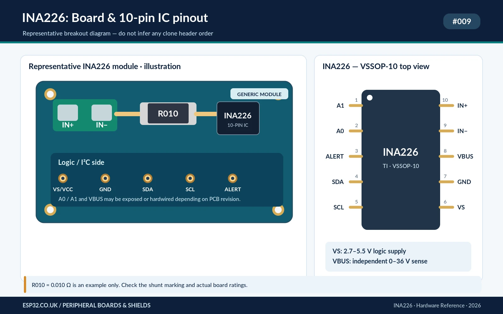
INA226 is a 10-pin VSSOP device. This is the actual pin assignment for the chip top view, not a promise that a generic module exposes the same pins in the same order. On a breakout, header locations and naming are PCB-manufacturer decisions.
| IC pin | TI pin name | Use |
|---|---|---|
| 1 | A1 | I²C address-selection input |
| 2 | A0 | I²C address-selection input |
| 3 | ALERT | Open-drain programmable alert output, may be omitted on inexpensive modules |
| 4 | SDA | I²C data, pull-up to logic voltage |
| 5 | SCL | I²C clock, pull-up to logic voltage |
| 6 | VS | INA226 logic supply, 2.7–5.5 V |
| 7 | GND | Common reference |
| 8 | VBUS | Independent positive bus-voltage input, 0–36 V |
| 9 | IN− | Shunt load-side sensing input |
| 10 | IN+ | Shunt source-side sensing input |
What is on a common INA226 module?
Commonly sold INA226 boards carry the small VSSOP chip, a low-ohmic resistor marked with its value, a VCC/VS and GND header, SDA/SCL, and screw terminals or pads for the high-current path. Some bring out VBUS, ALERT and A0/A1; others strap those pins internally. Do not assume a board advertised as “INA226 20A” uses the shunt assumed by your Arduino code. Even two outwardly similar boards can have different resistors and terminal layouts.
For the measurement path, the shunt carries the load current; the chip itself senses a small differential voltage across it. If a board uses a two-terminal power connector and the vendor says “VIN+ / VIN−”, this is not the same as the VS/VCC logic pin. A high-current current path must use terminals, conductors and a shunt designed for its load, including thermal rise and transient conditions.
INA226 I²C address: why two address pins give 16 options
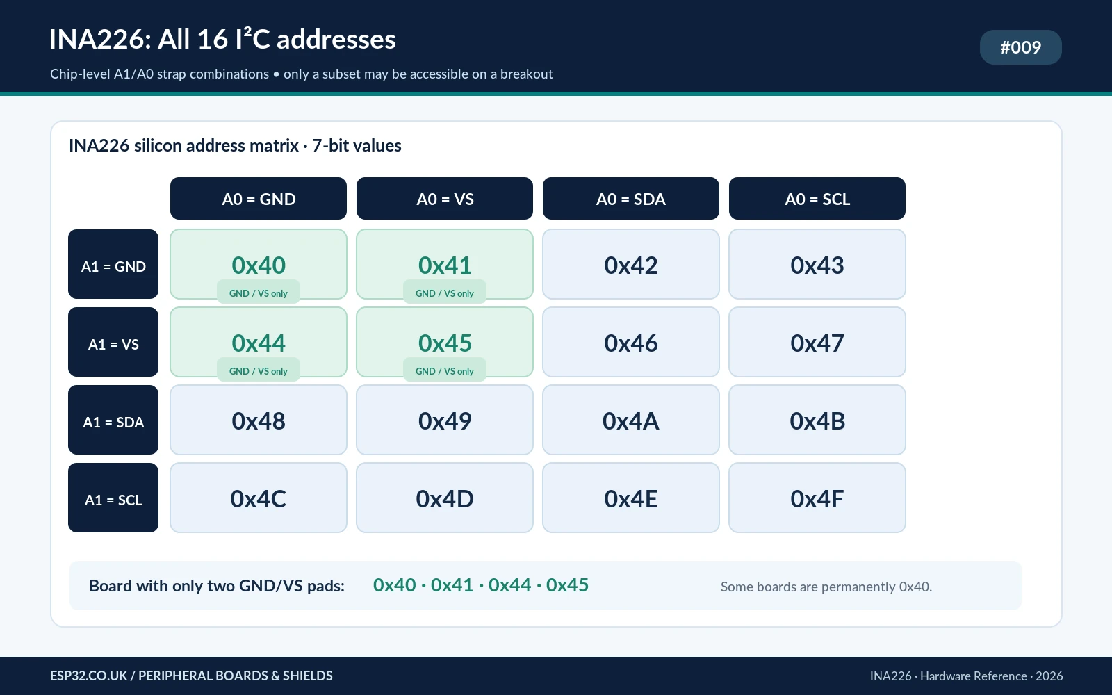
The INA226 has address inputs A0 and A1. Unlike a simple high/low binary jumper, the silicon accepts each pin tied to one of GND, VS, SDA or SCL, giving 16 combinations. Arduino Wire uses the seven-bit address, not an eight-bit bus address including the read/write bit.
| A1 | A0 | Address |
|---|---|---|
| GND | GND | 0x40 |
| GND | VS | 0x41 |
| GND | SDA | 0x42 |
| GND | SCL | 0x43 |
| VS | GND | 0x44 |
| VS | VS | 0x45 |
| VS | SDA | 0x46 |
| VS | SCL | 0x47 |
| SDA | GND | 0x48 |
| SDA | VS | 0x49 |
| SDA | SDA | 0x4A |
| SDA | SCL | 0x4B |
| SCL | GND | 0x4C |
| SCL | VS | 0x4D |
| SCL | SDA | 0x4E |
| SCL | SCL | 0x4F |
Physical solder-pad warning: a breakout with two ground-to-VS solder links may provide only 0x40, 0x41, 0x44 and 0x45. Some boards expose A0/A1 as header pins for all 16 possibilities, and some are fixed at 0x40. The availability and placement of bridges must be read from that PCB revision. Never draw or solder “universal INA226 address pads” that are not present.
High-side shunt circuit and functional schematic
Current follows the path DC supply + → shunt resistor → load +. Positive load current then produces a positive drop VSHUNT = V(IN+) − V(IN−). The INA226 measures this small differential voltage and a separate voltage on VBUS. For a typical high-side setup, connecting VBUS at the load-side rail reports the voltage actually delivered after shunt drop; some generic modules instead link VBUS to the supply-side rail. Read the board schematic or meter the continuity before trusting the reported voltage node.
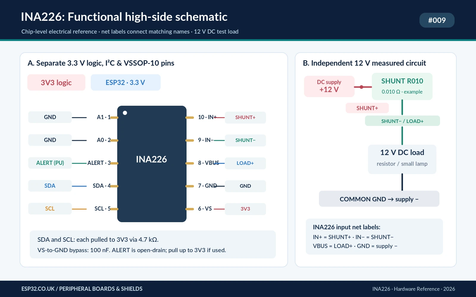
The minimum circuit uses a 0.1 µF ceramic bypass capacitor close to VS/GND, SDA and SCL pull-ups to 3.3 V, correctly strapped A0/A1, and Kelvin-sense traces or wires from IN+ and IN− to the shunt terminals. ALERT is an optional open-drain signal; if used, it needs a suitable pull-up to a compatible logic rail. Directly tying ALERT to an ESP32 without a correctly referenced pull-up may give unreliable interrupt levels.
VIN+ and VIN− are common breakout-label variants for the chip’s IN+ and IN− terminals. VBUS is not a current-carrying output; it is a high-impedance voltage-sense input. In low-side measurement the shunt location and VBUS routing differ, and low-side current sensing can introduce a small ground offset. This tutorial uses the easier high-side approach.
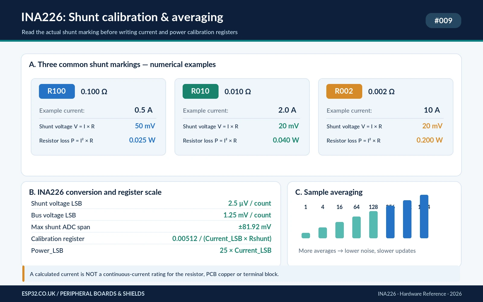
Shunt resistor markings: R100, R010 and R002 are different
A calibration value is only meaningful with the real resistor between the shunt-sense inputs. Read the component marking and vendor schematic. Common examples are shown below, but these are not promised component values for every module:
| Marking | Nominal resistance | Current corresponding to 81.92 mV | Shunt dissipation at example current |
|---|---|---|---|
| R100 | 0.100 Ω | 0.819 A theoretical | 0.5 A → 0.025 W |
| R010 | 0.010 Ω | 8.192 A theoretical | 2.0 A → 0.040 W |
| R002 | 0.002 Ω | 40.96 A theoretical | 10 A → 0.200 W |
The figures in the third column are obtained from I = 0.08192 / RSHUNT; they are not the safe current ratings of any breakout. A small PCB trace, screw terminal, sensing resistor, solder joint or cable can reach its thermal limit long before the theoretical 16-bit measurement full scale. For example, 8 A through 0.010 Ω dissipates 0.64 W in the shunt alone. Even when the resistor tolerates that power, the rest of a cheap module may not.
If the shunt is physically separate from the breakout, use Kelvin connections to keep load-carrying copper and connection resistance out of the differential measurement. For precision work, calibrate against a trusted meter and consider the shunt temperature coefficient and copper resistance. Resistive drop and self-heating are often larger errors than the IC gain specification.
ESP32 to INA226 wiring: one 12 V load example
| ESP32 or supply | INA226 signal | What it does |
|---|---|---|
| ESP32 3V3 | VS / VCC | INA226 digital supply only |
| ESP32 GND | GND | Shared reference with measured DC supply negative |
| ESP32 GPIO21 | SDA | I²C data, classic ESP32 example |
| ESP32 GPIO22 | SCL | I²C clock, classic ESP32 example |
| DC 12 V supply + | Shunt source end / IN+ | Positive DC source entering series shunt |
| Shunt load end | IN− and load + | Positive current from shunt into DC load |
| Load-side positive rail | VBUS (if routed separately) | Measures load-side bus voltage |
| 12 V supply − | Load − and shared GND | Completes DC load circuit; common measurement reference |
| Optional ESP32 GPIO27 | ALERT, 3.3 V pull-up | Open-drain fault/ready signal if exposed |
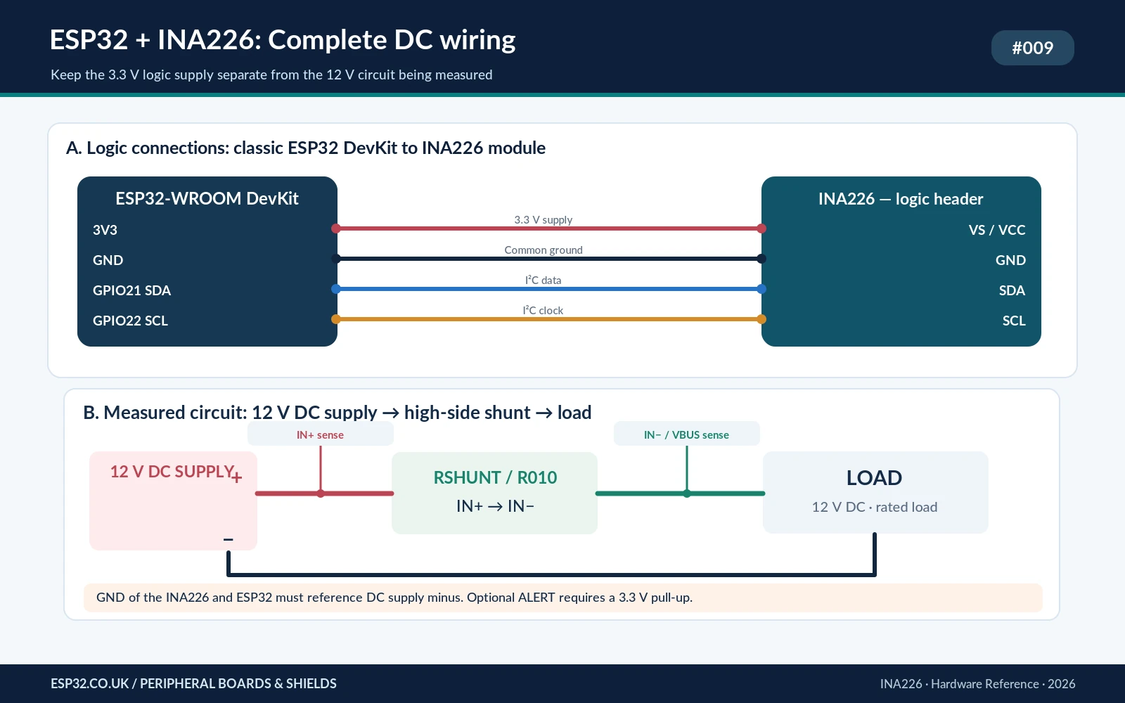
The ESP32 current does not flow through the 3V3 pin as part of the load measurement. Keep the load current path away from the ESP32 breadboard and connect only the appropriate sensor and reference wires. Start with a fused, current-limited low-voltage DC source and a resistive test load. The 0–36 V bus specification does not make a breakout safe for switching mains, high-energy batteries or unknown inductive surges.
Arduino IDE example: Rob Tillaart INA226 library
There is no widely used official Adafruit Arduino INA226 breakout library to rely on here. For this module, Rob Tillaart’s INA226 library is a sensible, documented Arduino choice. Install INA226 by Rob Tillaart in Arduino IDE Library Manager, and install Espressif’s ESP32 board support if needed. The example below follows the library’s current Wire.begin(), INA226(address), begin() and setMaxCurrentShunt() API. It is authored and documentation-checked but is not a claim of physical bench testing.
Before uploading: the example assumes a genuine R010 = 0.010 Ω shunt and a maximum expected current of 2 A. Change SHUNT_OHMS and MAX_CURRENT_A to match your hardware. An R100 board with a 2 A calibration target would exceed the ±81.92 mV differential input range and the library correctly flags that configuration as invalid.
#include <Arduino.h>
#include <Wire.h>
#include <INA226.h>   // Rob Tillaart INA226 library

constexpr int I2C_SDA = 21; // classic ESP32 DevKit example
constexpr int I2C_SCL = 22;
constexpr uint8_t INA_ADDRESS = 0x40;

// Check the actual SMD resistor marking on YOUR module!
// R010 = 0.010 ohm; R100 = 0.100 ohm; R002 = 0.002 ohm.
constexpr float SHUNT_OHMS = 0.010f;
constexpr float MAX_CURRENT_A = 2.0f;

INA226 ina(INA_ADDRESS);

void setup() {
  Serial.begin(115200);
  delay(300);
  Wire.begin(I2C_SDA, I2C_SCL);
  Wire.setClock(100000);

  if (!ina.begin()) {
    Serial.println("INA226 not detected at 0x40");
    Serial.println("Check 3.3V, GND, SDA, SCL and A0/A1.");
    while (true) delay(1000);
  }

  // Calibration is REQUIRED for meaningful current and power.
  const int calError = ina.setMaxCurrentShunt(
      MAX_CURRENT_A, SHUNT_OHMS, false);
  if (calError != 0) {
    Serial.printf("INA226 calibration error: 0x%04X\n", calError);
    while (true) delay(1000);
  }

  // 16 averaged readings; all conversion times otherwise default.
  ina.setAverage(INA226_16_SAMPLES);
  Serial.println("INA226 initialised and calibrated");
}

void loop() {
  const float busV   = ina.getBusVoltage();    // VBUS to GND
  const float shuntV = ina.getShuntVoltage();  // IN+ minus IN-, V
  const float amps   = ina.getCurrent();       // A
  const float watts  = ina.getPower();         // W

  Serial.printf("VBUS: %.3f V | shunt: %.3f mV | "
                "I: %.4f A | P: %.3f W\n",
                busV, shuntV * 1000.0f, amps, watts);
  delay(500);
}
Open the serial monitor at 115200 baud. The program reports VBUS, VSHUNT, current and power. These readings are only meaningful when the shunt and bus wiring are correct, the calibration succeeded, and the device has completed a conversion. Setting larger sample counts smooths fluctuating values but slows the update rate; do not use a half-second print interval as proof that every print contains a new averaged conversion.
Example output and sanity checks
INA226 initialised and calibrated
VBUS: 11.986 V | shunt: 10.000 mV | I: 1.0000 A | P: 11.986 W
VBUS: 11.985 V | shunt: 10.003 mV | I: 1.0003 A | P: 11.989 W
The serial lines above are illustrative, not measured test results. With a 0.010 Ω shunt, an observed 10 mV drop corresponds to approximately 1 A. As a separate check, measured current should approximately equal VSHUNT / RSHUNT and power should approximately equal VBUS × current. The two displayed values may not exactly match because separate conversions, digital calibration, quantization and rounding all contribute.
INA226 calibration math and register-level accuracy
The INA226 measures a signed 16-bit shunt-voltage register and a positive bus-voltage register. Their fixed step sizes are 2.5 µV per bit and 1.25 mV per bit respectively. The current and power registers must be scaled using the actual shunt resistor value:
V_shunt (volts) = shunt_register_signed * 2.5e-6
V_bus   (volts) = bus_register_unsigned * 1.25e-3
I_shunt (amps)  = V_shunt / R_shunt

Current_LSB (A/bit) ≳ expected_max_current / 32768
Calibration_Register = 0.00512 / (Current_LSB * R_shunt)
Power_LSB (W/bit) = 25 * Current_LSB
TI’s calibration equation contains the constant 0.00512, while current-LSB selection establishes the current-register scaling. The library handles the register arithmetic once you give it the shunt resistance and target current. Avoid copying a ready-made INA219 calibration constant: the INA219 has a different calibration scale and measurement architecture.
Averaging, ALERT and configuration choices
The INA226 can average 1, 4, 16, 64, 128, 256, 512 or 1024 readings. It also offers independently programmable shunt- and bus-voltage conversion times. Faster settings respond better to changes; slower conversions and averaging reduce noise but delay detection. For a battery monitor or static laboratory supply, 16 or 64 averaged readings may be suitable. Fast overcurrent protection needs more careful latency analysis than a simple loop that polls every 500 ms.
The active-low ALERT output is open-drain and can signal a bus/shunt threshold, power limit or conversion-ready condition. It is not a power-interrupting relay. For protection it must connect to appropriate controller logic, which must then actuate a properly rated switch. Set the alarm mask and threshold through the library or registers, fit a 3.3 V pull-up, and test fail-safe behavior before relying on this for equipment protection.
INA226 versus INA219: which sensor belongs in your project?
| Feature | INA219 | INA226 |
|---|---|---|
| DC bus measurement | Up to 26 V | Up to 36 V |
| Conversion resolution | 12-bit ADC class | 16-bit ADC class |
| Current measurement | Shunt, gain/range selections | Shunt with programmable calibration and conversion averaging |
| Voltage sense | Bus voltage based on chip topology | Independent VBUS sense input |
| Addressing | 16 theoretical, module-dependent | 16 theoretical, module-dependent |
| Typical projects | Basic ESP32 power checks | More precise supply, solar, battery and DC rail monitoring |
The INA226 is not automatically better in every application: a correctly sized shunt, wiring, thermal design, calibration and quality power supply are more important than the headline bit count. For an existing comparison, see INA219 vs INA226 vs INA260. For ESPHome/Home Assistant integration, see INA226 with ESP32 and ESPHome and INA219/INA226 on ESP32 for Home Assistant.
Troubleshooting INA226 problems
| Symptom | What to check first |
|---|---|
| No device found at 0x40 | 3.3 V on VS, common GND, SDA/SCL orientation, presence of pull-ups; run an I²C scanner for addresses 0x40–0x4F. |
| Voltage works but current and power are 0 | Run the required current calibration; verify the shunt is connected between IN+ and IN− and carries load current. |
| Current differs by factor 10 or 50 | R100 versus R010 versus R002 module resistor, incorrect shunt-ohm parameter or a parallel conduction path bypassing the shunt. |
| Wrong sign for current | Swap the shunt sense polarities or correct the software assumption, after safely disconnecting power. |
| Bus voltage looks like supply voltage instead of load voltage | VBUS wired to source side rather than load side or board has a factory bridge; verify continuity and board schematic. |
| Current saturates or calibration error appears | I × R exceeds ±81.92 mV input span; lower max-current setup or redesign shunt for the actual application. |
| Readings noisy or wander | Short Kelvin-sense connections, stable ground, correct shunt and suitable averaging/conversion time; avoid large high-current return loops. |
| I²C fails after connecting load supply | No shared reference, high-current ground bounce, inductive transients or 5 V logic pull-ups on unprotected ESP32 pins. |
Frequently asked questions
Can I use INA226 with a 24 V or 36 V DC supply?
Yes, within the device’s 0–36 V bus-measurement operating range and the actual breakout’s component and insulation ratings. Keep its VS logic power at 3.3 V for ESP32. A nominal 36 V supply can produce surges beyond 36 V, so reserve voltage margin and protect against transients.
Does the INA226 measure AC mains current?
No. This is a DC current/shunt and voltage monitor. Do not connect its breakout terminals directly to household mains or other hazardous high-energy circuits.
What does R002 mean?
The resistor is nominally 0.002 Ω, or 2 mΩ. Its low resistance expands the theoretical current span but reduces the shunt signal at low current and creates demanding PCB, thermal and Kelvin-sensing requirements. Never interpret the 40.96 A full-scale calculation as a safe board rating.
How many INA226 boards can share one I²C bus?
The silicon supports 16 addresses from 0x40 through 0x4F. However, your physical breakout might allow four, two, or only one of them. For fixed-address boards, a TCA9548A I²C multiplexer can put duplicate addresses on separate branches.
Can I read voltage without calibrating the current channel?
Yes. The bus and shunt voltage registers are direct measurements with fixed LSB values; current and power are dependent on the calibration register. A completely missing or open shunt still makes the current measurement meaningless.
References
- Texas Instruments INA226 datasheet, Rev. C, August 2026 — pin numbers, address table, register ranges, calibration and application circuits.
- Texas Instruments product information — active product and operating specifications.
- Rob Tillaart INA226 Arduino library — initialization, calibrated current readings and API.
- esp32.co.uk/ INA226 ESPHome tutorial — integration and Home Assistant use cases.
Hardware note: INA226 modules come from multiple vendors. The chip functions and programming are defined by Texas Instruments; jumper placement, onboard shunt value, shunt power rating, voltage-sense bridge, header order and trace width are breakout-specific. Verify your actual module before applying power.