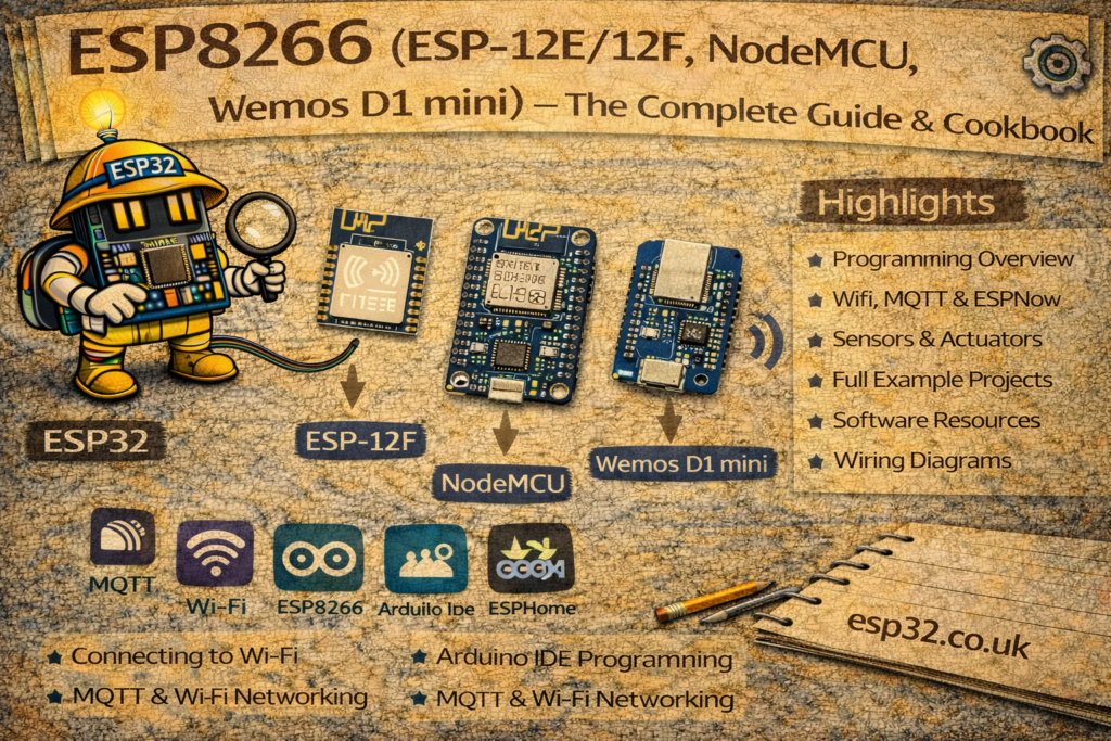
This guide explains the most common ESP8266 variants (ESP-01, ESP-12E/F, NodeMCU and D1 mini) and shows their pinouts, safe GPIOs, and boot-sensitive pins to avoid.
The ESP8266 started life as a tiny Wi-Fi module but quickly became a full microcontroller platform. Under the metal cans, almost all modules use the same chip (ESP8266EX) – what changes is:
- How many GPIO pins are brought out
- Antenna type (PCB vs ceramic vs u.FL)
- Form factor (bare module vs dev board)
This guide covers the most common variants you’ll actually meet:
- ESP-01 / ESP-01S – 8-pin “stick” module
- ESP-12E / ESP-12F (and ESP-07) – 22-pad SMD modules
- NodeMCU dev board – ESP-12E on a USB dev board
- Wemos D1 mini – small, breadboard-friendly dev board
And we’ll summarise pinouts and which pins are “safe” to use.
⚠️ All ESP8266 boards are 3.3 V only on their GPIOs. Feeding 5 V directly into any GPIO will kill the chip.
1. ESP-01 / ESP-01S – the tiny 8-pin classic
The ESP-01 is the original “blue board” most people saw first: a tiny module with only 8 pins broken out. It’s cheap and widely used in legacy designs.
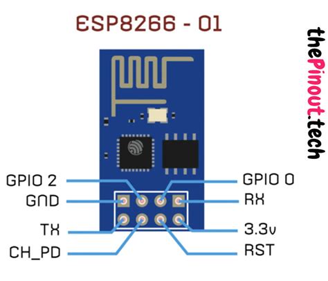

Typical pinout (viewed from top, pins pointing down)
| Pin | Name | Function |
|---|---|---|
| 1 | GND | Ground |
| 2 | GPIO2 | I/O, also affects boot mode |
| 3 | GPIO0 | I/O, boot-mode / flash pin |
| 4 | RXD0 | UART0 RX |
| 5 | TXD0 | UART0 TX |
| 6 | CH_PD / EN | Chip enable (pull HIGH to run) |
| 7 | RST | Reset (active LOW) |
| 8 | VCC | 3.3 V power |
Practical notes:
- Usable GPIOs in normal projects: GPIO0, GPIO2 (both have boot-mode roles)
- To flash firmware, you usually:
- Hold GPIO0 LOW at reset → enter bootloader
- Use TXD0/RXD0 as serial connection
- Very limited number of I/O pins makes ESP-01 a pain for bigger projects. Great as a Wi-Fi modem or for very small nodes.
2. ESP-12E / ESP-12F (and ESP-07) – full GPIO access
Modules like ESP-12E, ESP-12F and ESP-07 expose almost all usable pins of the ESP8266EX. They’re metal-shielded SMD modules used on dev boards like NodeMCU.
They all share a very similar core pinout; ESP-12E/F adds an extra bottom row mainly for flash pins.
High-level features of the ESP-12 class:
- 17 GPIOs total on the chip, ~11–13 usable on typical modules
- 1× 10-bit ADC (A0)
- PCB antenna (ESP-12), ceramic antenna (ESP-07)
Typical ESP-12E pin groups:
- Power & control:
VCC,GND,EN/CH_PD,RST - UART0:
TXD0(GPIO1),RXD0(GPIO3) – default programming / logging port - SPI flash pins:
GPIO6–GPIO11– used internally, don’t touch - General GPIOs:
GPIO0, 2, 4, 5, 12, 13, 14, 15, 16 - ADC:
TOUTorADC0– 0–1.0 V max
Example bare ESP-12E pinout:
- “Safe” GPIOs most people use:
- GPIO4, GPIO5, GPIO12, GPIO13, GPIO14 → best general I/O
- GPIO16 for deep-sleep wake (connected to
RST)
- Boot-sensitive pins:
- GPIO0, GPIO2, GPIO15 control boot mode – must be at the right level on reset.
- GPIO1/3 used for UART – toggled during boot.
3. NodeMCU (ESP8266 dev board) – ESP-12E on a USB PCB
NodeMCU boards like NodeMCU v1.0 (ESP-12E) take an ESP-12 module and add:
- USB-to-serial (CP2102/CH340)
- 3.3 V regulator
- Auto-reset / auto-flash circuitry
- Breadboard-friendly pins labelled D0, D1, D2… instead of raw GPIO numbers
Typical NodeMCU ESP-12E dev board pinout:
| Board label | ESP8266 GPIO | Notes |
|---|---|---|
| D0 | GPIO16 | No PWM, wake from deep sleep only |
| D1 | GPIO5 | I²C SCL (by convention) |
| D2 | GPIO4 | I²C SDA (by convention) |
| D3 | GPIO0 | Boot mode pin, pulled-up |
| D4 | GPIO2 | Boot mode pin, on-board LED on many |
| D5 | GPIO14 | HSPI CLK |
| D6 | GPIO12 | HSPI MISO |
| D7 | GPIO13 | HSPI MOSI |
| D8 | GPIO15 | Boot mode pin, pulled-down |
| RX | GPIO3 | UART0 RX (Serial) |
| TX | GPIO1 | UART0 TX (Serial) |
| A0 | ADC0 | 0–1.0 V (often via on-board divider) |
Good defaults on NodeMCU:
- I²C →
D2 (GPIO4)SDA,D1 (GPIO5)SCL - SPI →
D5 (GPIO14)SCK,D6 (GPIO12)MISO,D7 (GPIO13)MOSI,D8 (GPIO15)CS - Avoid using
D3 (GPIO0),D4 (GPIO2),D8 (GPIO15)for things that pull hard HIGH/LOW at boot.
4. Wemos D1 mini – small and popular
The Wemos D1 mini is a very compact dev board with an ESP-12 module, micro-USB and 3.3 V regulator. It exposes 11 usable GPIOs and is extremely popular in DIY and Home Assistant projects.
Typical D1 mini pin mapping:
| Label | GPIO | Typical use |
|---|---|---|
| D0 | GPIO16 | Deep sleep wake, no PWM |
| D1 | GPIO5 | I²C SCL |
| D2 | GPIO4 | I²C SDA |
| D3 | GPIO0 | Boot pin, input w/PU |
| D4 | GPIO2 | Boot pin, on-board LED |
| D5 | GPIO14 | SPI SCK |
| D6 | GPIO12 | SPI MISO |
| D7 | GPIO13 | SPI MOSI |
| D8 | GPIO15 | Boot pin (pulled-down) |
| RX | GPIO3 | UART0 RX |
| TX | GPIO1 | UART0 TX |
| A0 | ADC0 | 0–1.0 V (via onboard divider often ~3.3→1.0) |
Notes:
- Only one ADC channel (A0).
- D0 (GPIO16) can’t do I²C or SPI, and has limitations on interrupts/PWM.
- Don’t tie
D3, D4, D8to random stuff that changes the boot levels.
5. Other ESP8266 module variants (brief overview)
There are more SMD modules, but they’re all the same chip plus different antennas / footprints:
- ESP-05 – tiny module with just UART pins and power (like ESP-01 but even more limited).
- ESP-07 – similar pinout to ESP-12 but with ceramic antenna and u.FL connector.
- ESP-201 / ESP-14 – older / less common modules with their own pinouts.
The main differences are:
- How many GPIOs are broken out
- Antenna type (PCB vs ceramic vs external connector)
- Footprint and shield size
The actual SoC (ESP8266EX) and its GPIO roles are the same across all of them.
6. Safe GPIOs vs “tricky” GPIOs (boot pins)
Because of boot-mode strapping, some pins must be at defined levels during reset. The classic rule from the ESP8266 pinout references:
Boot strapping pins:
- GPIO0
- GPIO2
- GPIO15
Valid boot from flash requires:
GPIO0 = HIGHGPIO2 = HIGHGPIO15 = LOW
So:
- Don’t pull GPIO0 or GPIO2 hard LOW at boot.
- Don’t pull GPIO15 HIGH at boot.
- You can use them after boot, but avoid big loads or things that force the wrong level during reset.
Generally safe GPIOs on ESP-12 / NodeMCU / D1 mini:
GPIO4, GPIO5, GPIO12, GPIO13, GPIO14, GPIO16